


The SPADIC Project Website
Welcome to the official SPADIC project website. On the following pages you will find very different kinds of information about the SPADIC project in general and on the SPADIC ASIC in particular.
What is SPADIC?
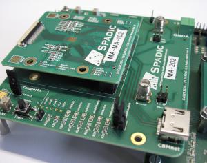
The SPADIC project relates to the name of the SPADIC readout chip (Self-triggered Pulse Amplification and Digitization asIC) which is intended to read out and process small electrical detector signals on a single piece of silicon. The latest SPADIC version 1.0, which is actually the 6th but first full-blown prototype, is a 32-channel mixed-signal readout chip dedicated for the readout of the transition radiation sub-detector (TRD) that will be part of the future CBM heavy-ion experiment at GSI/FAIR. SPADIC 1.0 provides low-noise and low-power analog pre-amplification, 8 bit digitization, IIR signal processing, self-triggered hit detection, neighbor readout, full pulse recording, meta data generation, synchronization mechanisms, and various other features.