


Some history of SPADIC in pictures
|
||||
|
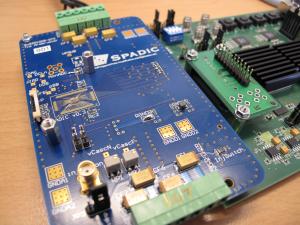
October 2010: A picture of the SPADIC v0.3 setup. The chip is directly wire-bonded onto the blue (Rev.2)
front-end board. The front-end board is plugged on the Susibo (Rev.2) FPGA readout board. The small
connector on the left is used to connect the 8 available channels to the detector. This setup
has been used in the first CERN testbeam in 2010 with different TRD chambers from Münster and
Frankfurt.
|
|||