Aktuelle Forschungsprojekte am Lehrstuhl - nur in Englisch !
This page contains short overviews of our ongoing research projects and some past projects (marked as 'done'). We tried to write the text on a level which can - hopefully - also be understood by non-experts in the field. Note that high resolution images are generated when clicking on most pictures.Background:
Optical photons are omnipresent in everyday life but also in science.
In many cases, we 'see' only what is going on because we observe / detect photons.
It is therefore an obvious goal to increase the sensitivity of photo detectors, so that they can see very low light levels.
The ultimate limit is the observation of single photons. This is not really possible with normal 'cameras'
which just collect the signal charges produced by the absorbed photons because the charge produced by just one
photon is too small (compared to electronics noise).
A detector which is able to achieve this goal is the so-called 'Single Photon Avalanche Diode', the SPAD.
These devices are made out of silicon. A photon impinging onto the surface penetrates into the silicon (sometimes it is reflected)
for a few micrometers (depending on wavelength) and is then absorbed and produces a single free electron
(this does not always happen so that the devices have a reduced 'quantum efficiency' of several 10%).
By applying a 'bias' voltage of several 10 V across a thin surface layer, a high electric field is generated.
This field accelerates the electron so that it can hit other atoms so strongly that further electrons are generated,
which are accelerated again and so on, so that an avalanche develops.
The overall charge in such an avalanche is so high that it is rather easy to measure electronically.
After the avalanche has discharged the device, it must be recharged again to the bias voltage,
which takes some time, so that the SPAD is 'blind' for some time after it has 'fired'.
This basic operation principle is used in different device types.
In order to cover larger areas, large SPADs can (and have been) build, but such 'APD' devices are quite
delicate to operate and the recharging time after a hit makes the full area insensitive.
A more popular approach is a clever parallel connection of many (many 1000) small SPADs (with some 10 μm pitch).
These so called 'Silicon Photomultipliers' (SiPMs) have just 2 pins.
We have used such SiPMs to build PET detection modules, and invented
a position sensitive variant.
When multiple photons hit a SiPM , several SPAD cells can fire and the signals add up at the output. Unfortunately, they are
overall strongly attenuated by the presence of the many other cells.
An amplifier is therefore required to detect the hit (we have designed such amplifier chips, see chapter PETA below).
A SiPM therefore always needs an extra electronics chip (often in close vicinity) to amplify and process the signal.
This requires power, cooling etc. and is a drawback in many applications.
A rather obvious solution is to manufacture the SPADs and the transistors required for the electronics on the same piece of silicon.
Such devices are often called 'digital SiPMs' (DSiPM).
They offer the possibility to integrate a readout and data processing into the devices to do many interesting things, see below.
We see a very high potential in such devices and have worked on many different variations since several years.
A challenge in the design of DSiPMs is that the area occupied by the electronics is not sensitive to photons (only the SPADs are), so that the
photon detection efficiency ('PDE') is reduced. It needs clever designs with a minimum number of transistors and clever arrangement
of the devices to maximize the SPAD area defining the 'fill factor'.
The fabrication of good SPADs (with good quantum efficiency and a low rate of noise hits)
requires additional processing steps and 'tricks' which are not available in most semiconductor fabs.
Only few vendors provide technologies which combine both devices, and many are hardly accessible for small groups or too expensive for us.
We are using the technology of the Fraunhofer Institute for Microelectronic Circuits IMS in Duisburg,
a 350 nm process with 4 metal layers.
Project Description:
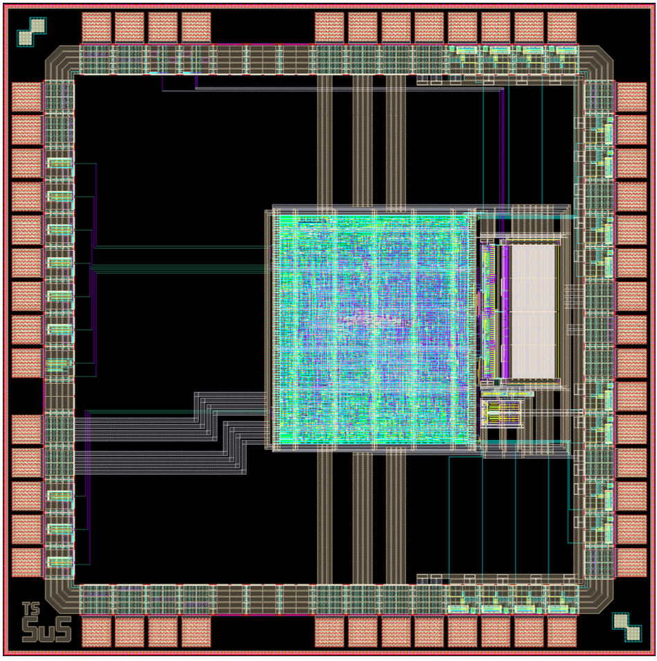
The chips presented in this section can make two-dimensional images, like a classical camera, but with single photon sensitivity!
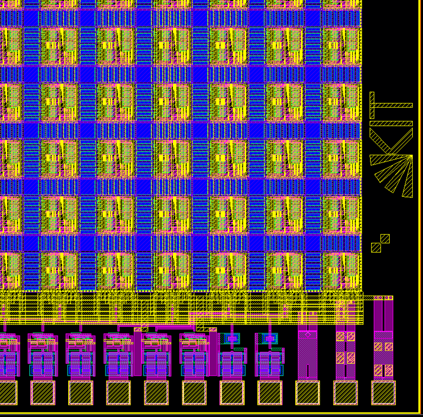
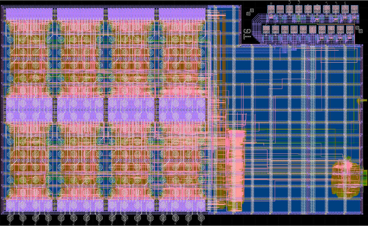
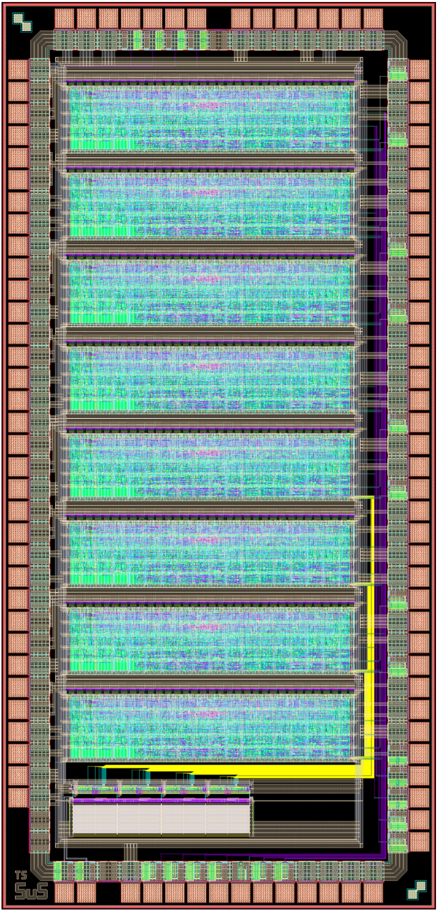
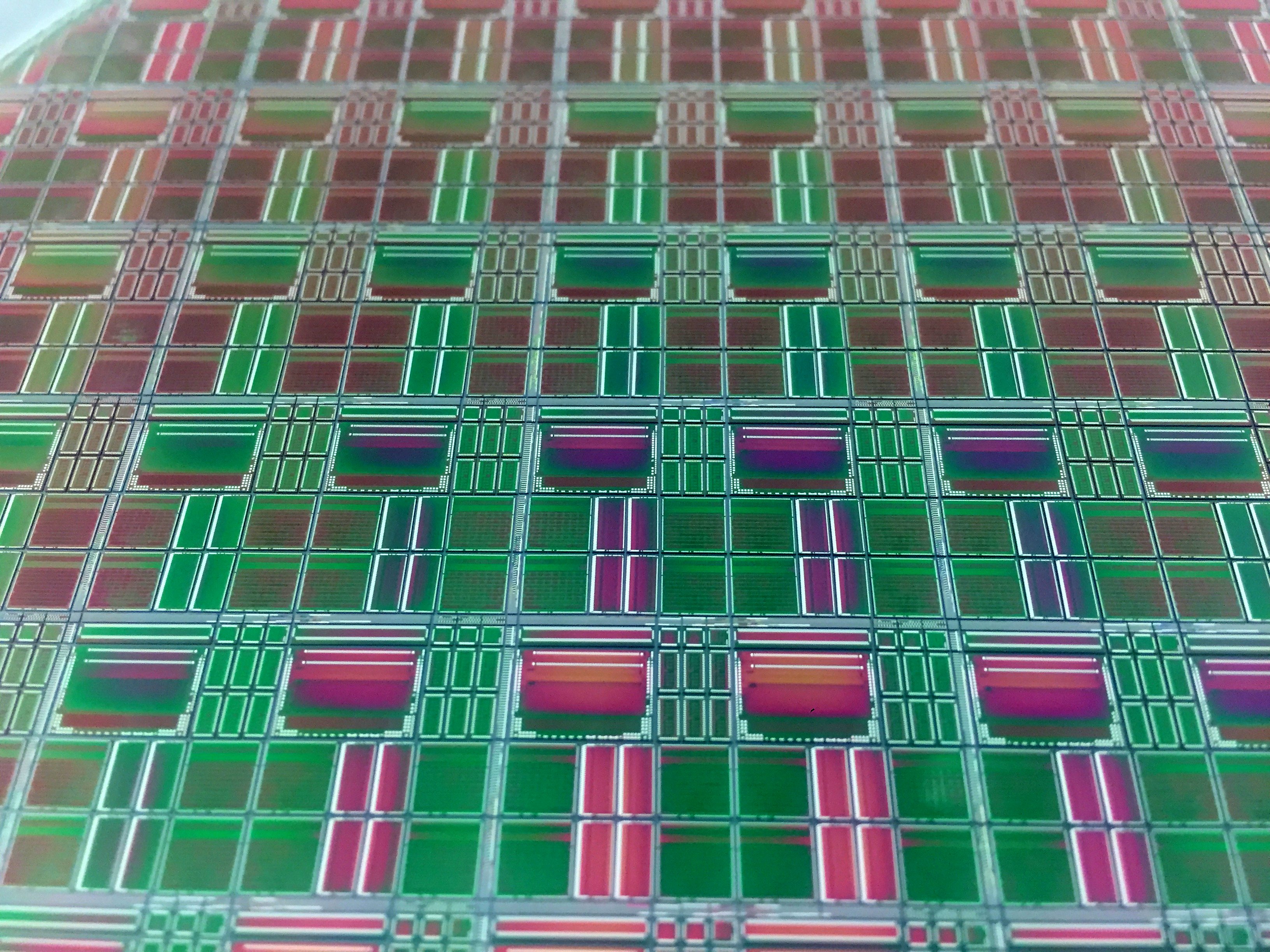
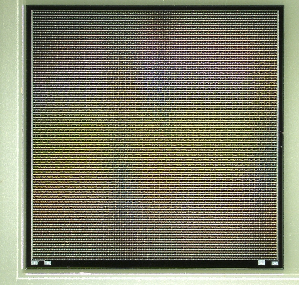
The active area is divided into pixels of roughly 50×50μm² with a good fill factor of more than 50% (photograph and layout upper right).
These pixels are arranged in a matrix of ~100×100 elements (photograph upper left). The electronics in the pixels observes the SPAD for
a certain time window (down to some 10 ns) and detects either a hit or no hit. The 1/0 information of all pixels is then shifted
to the bottom of the chip and from there out of the chip through one or several digital signal lines.
This process is very fast, so that several 100.000 images per second can be recorded, each delivering a binary image with 1/0 information.
These images can be overlaid offline to form gray scale images.
One started project is the 2D measurement of fluorescence light from micro-biological samples (in cooperation with KIT).
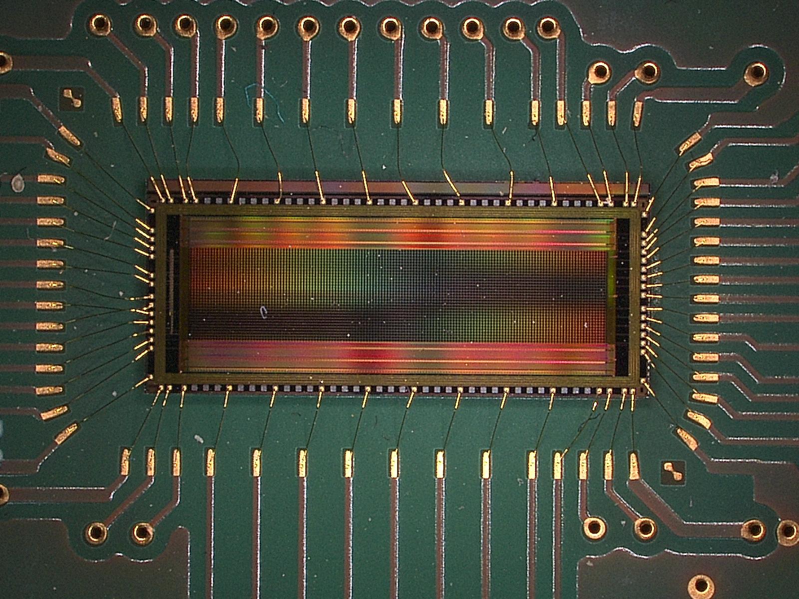
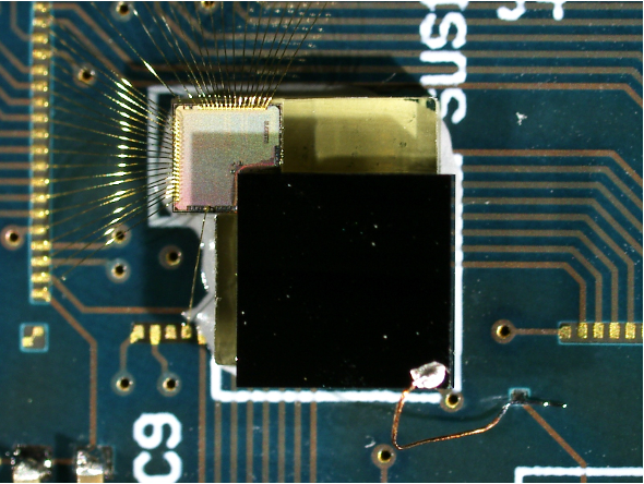
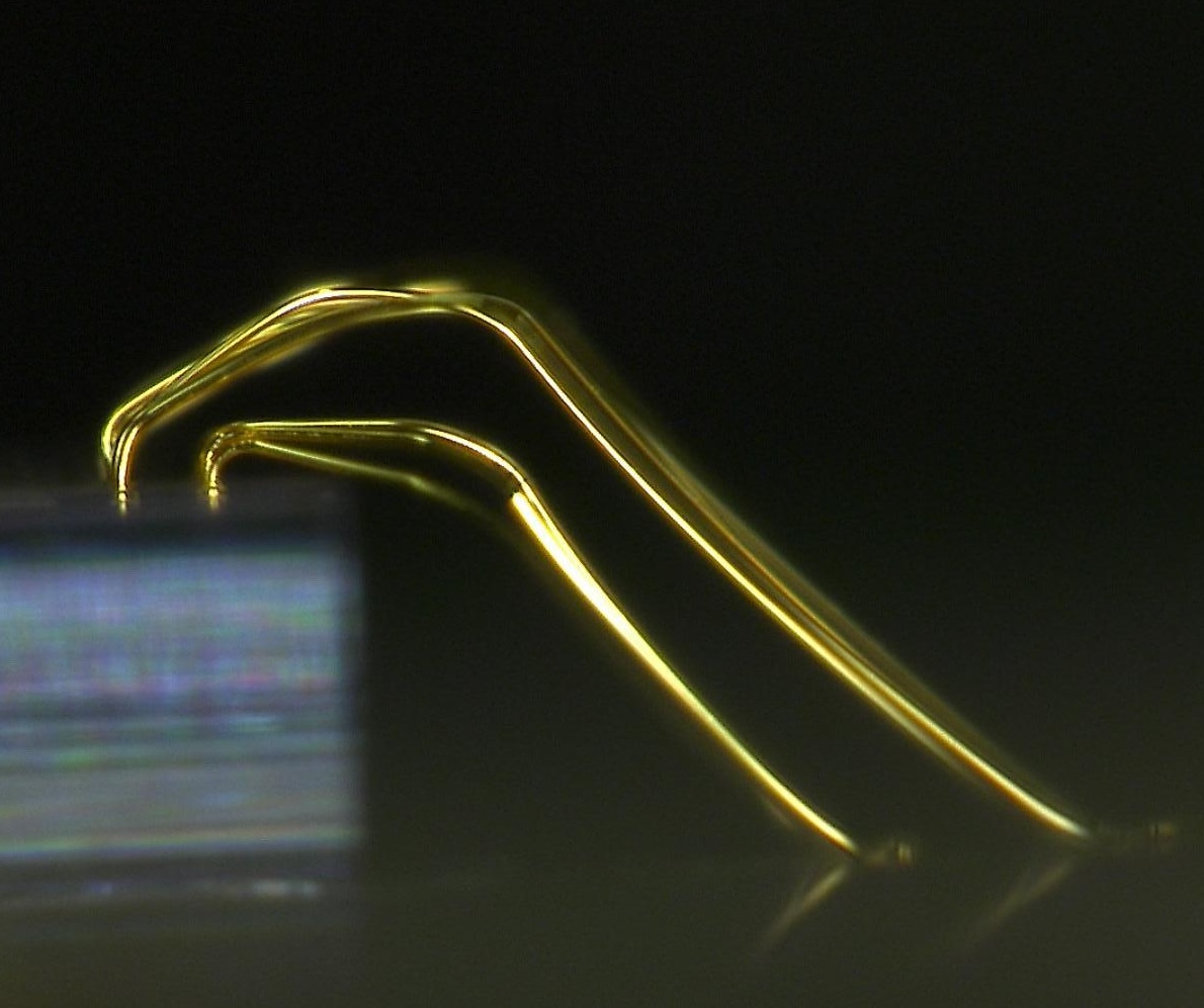
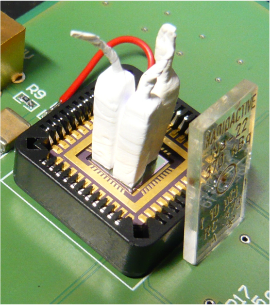
Image Descriptions: The photograph (middle, left) shows a chip connected to a printed circuit board with tiny 'wire-bonds'. In this case, the chip sits on a white Peltier cooler to control (and lower) its temperature, which affects a lot the rate of noise hits ('dark counts'). Another board (with a later and even larger chip version) is shown below where the 'wire-bonds' are mechanically protected by a 3D printed cover. For tests, such a board was used to image an optical test pattern with single photons (bottom right) or to detect the photons from an array of scintillating crystals placed on top. This chips of our 'IDP' family are being used by a wide range of projects to image single photons, like fluorescence imaging in biology, measurement of Rayleigh scatter or for electron detection with 3D printed scintillators.
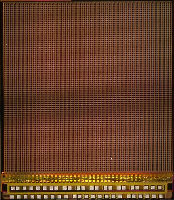
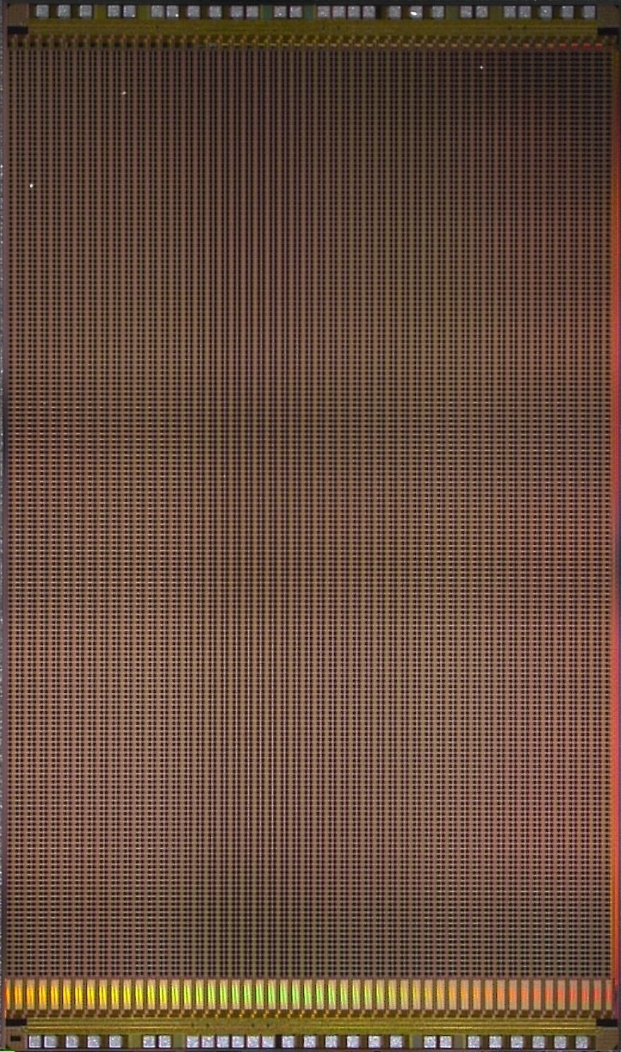
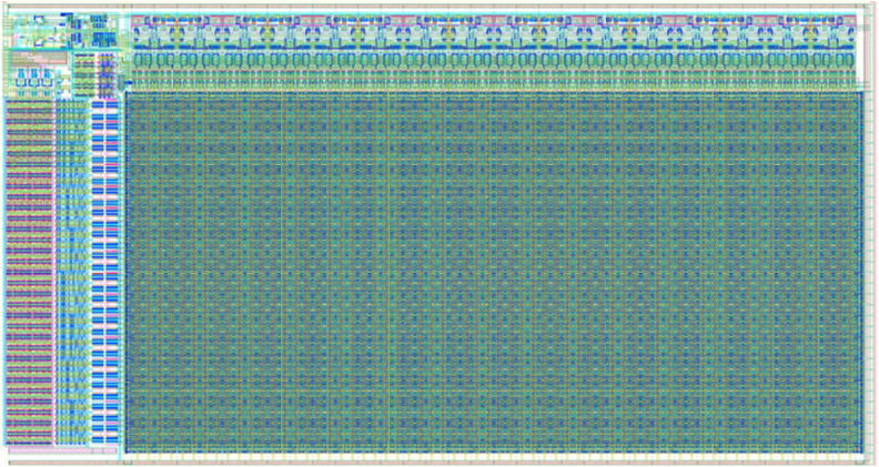
SPAD imaging chip 'IDP2'. The imaging matrix has an area of ~5×5 mm²
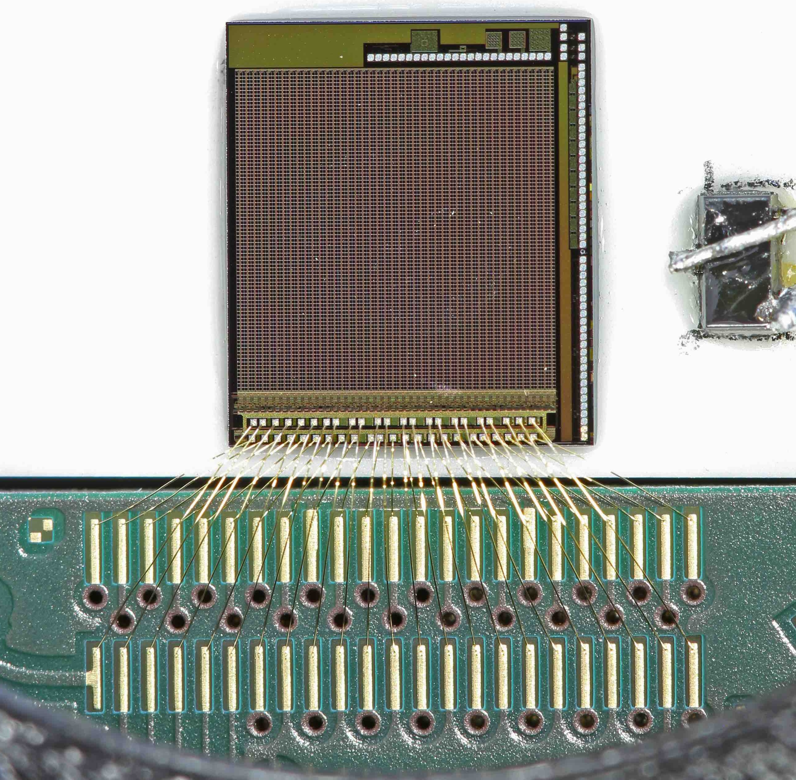
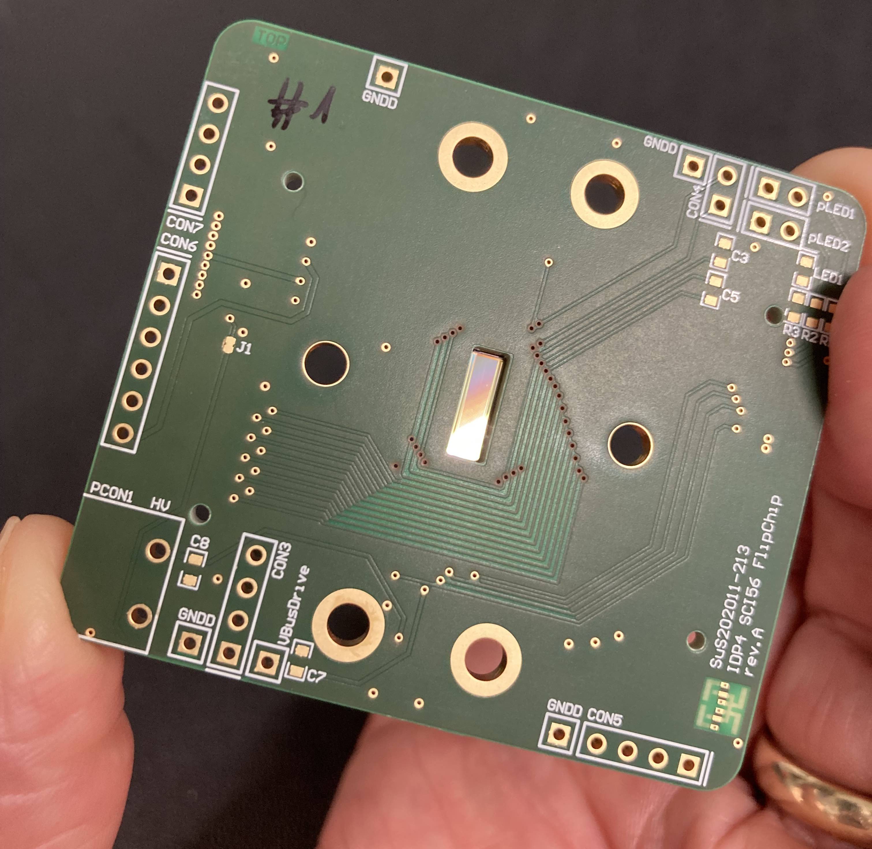
IDP4 Chip on a Peltier cooling plate wire bonded to a PCB.
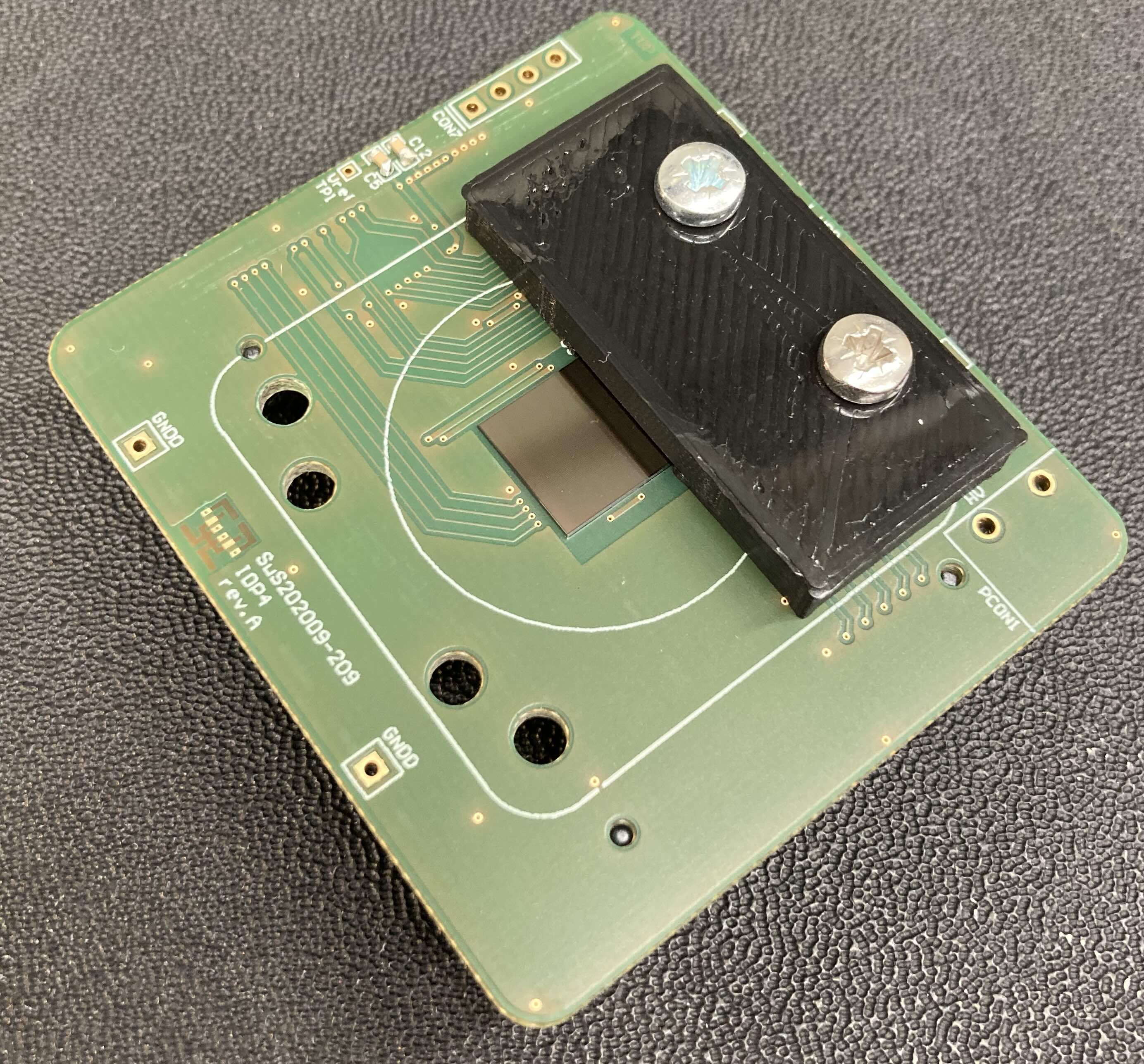
IDP4 Chip on PCB. The wire bonds are protected by a 3D-printed cover.
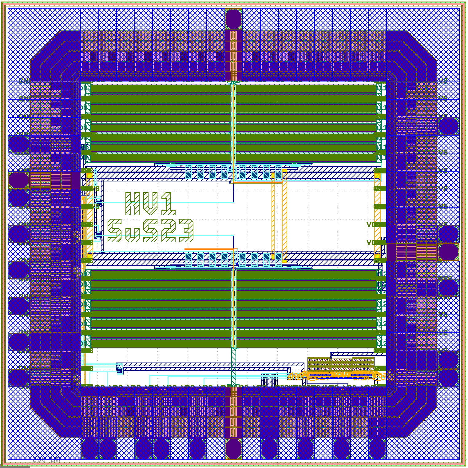
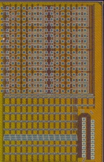
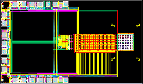
Zoom to Pixels. The large areas are the photo sensitive SPADs, the electronics is under to yellow metal traces.
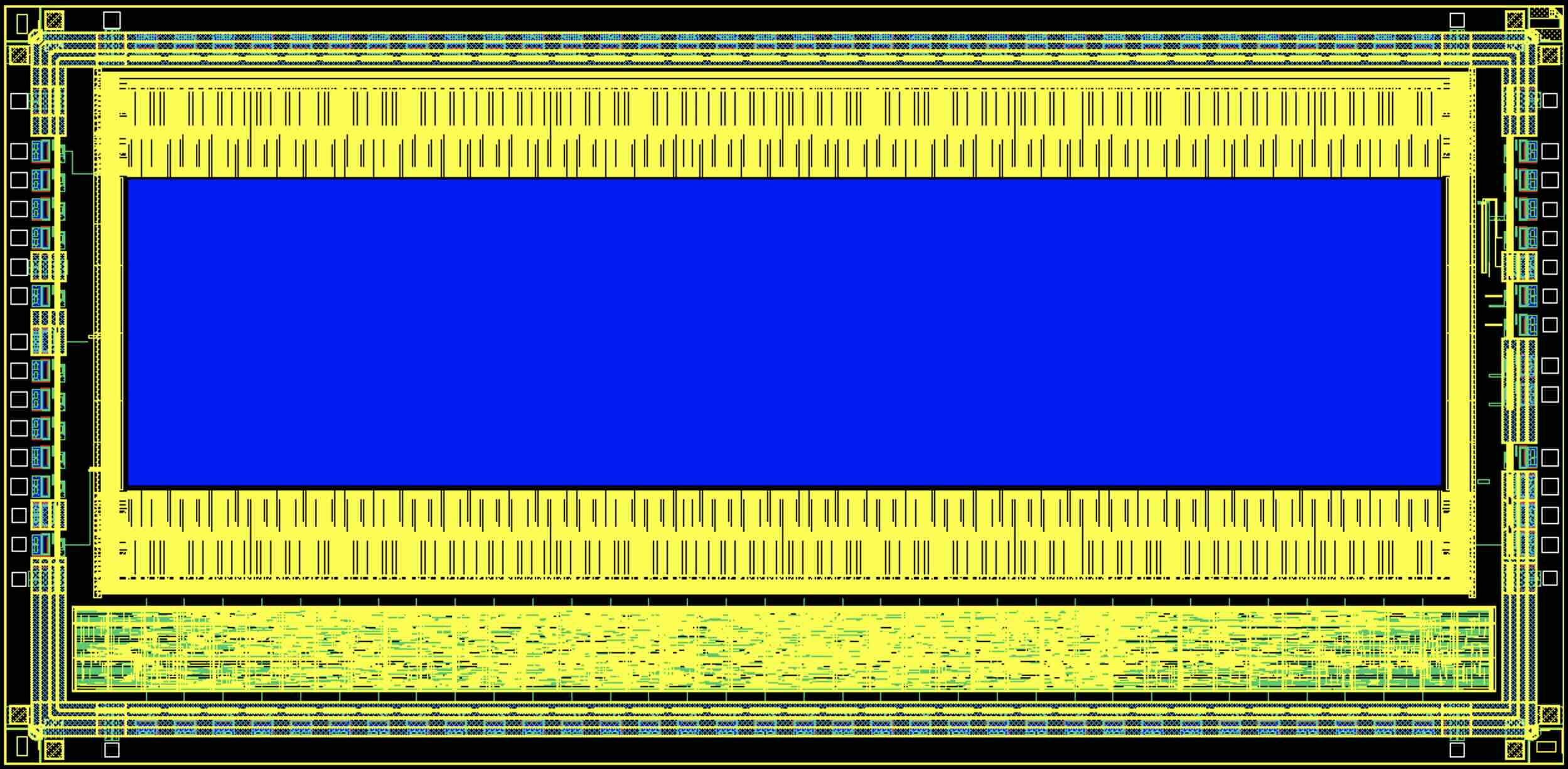
Layout view of a pixel pair of the same chip as above. The uppermost (power) metal layer is not shown.

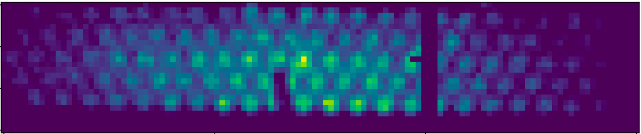
Measured scintillation Event from a segmented LYSO array standing on a IDP chip.
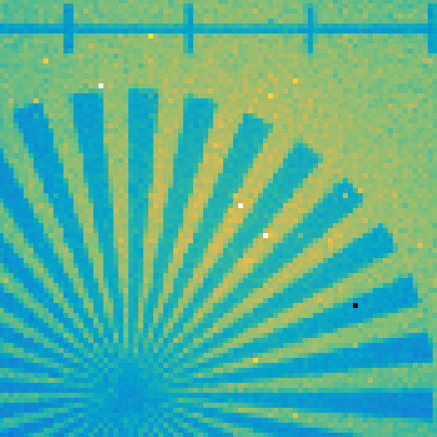
Test pattern imaged onto an IDP chip and illuminated with single photons.
Background:
Light can be sent from one position to another using optical fibers. The diameter of their light-carrying part is only some 10-100 μm.
Such fibers are used in some applications to collect light from a physical processes in the 'inner part' of an experiment and bring it further away
to an area (with more space or less particle radiation) where the photons are detected. Examples are tracking detectors for particles in high-energy physics
or medical radiation monitoring or 'calorimeters' measuring particle energies in high-energy physics.
These detectors often use 'scintillating' fibers which produce small amounts of light when traversed by charged particles.
The light - often only few photons - in the fibers must be detected at its end. SiPMs as described in the previous section are one possibility.
As they come in a fixed geometry, each fiber end must be placed exactly on top of one SiPM, which makes the assembly very delicate.
As always with SiPMs, additional low noise amplifier chips are needed to convert the tiny signals of the SiPM to digital information.
Project Description: We propose to use digital SiPM to simplify such systems: The photo sensitive part of the chip consists of an array of densely packed small SPADs. The fibers can be placed at arbitrary positions, as illustrated in the drawing (upper left). The chip is then programmed such that just the SPADs under one fiber (colored in the figure) are assigned to a 'group'. The number of SPADs firing in such a group is added up electronically and the information of the number of hits is sent off-chip. Because the internal SPAD signals are high, no further amplifier chip is needed. This is described in more detail in this publication. In the present chip, each SPAD group is electronically connected (by appropriate programming of the chip) to one of many digital outputs. The number of hit SPADs is encoded as the duration of a digital pulse (some 100 ns). One connection is therefore needed per group. A new chip, presently under fabrication, contains a logic which converts the pulse-widths of all groups to digital values and sends them off-chip on a single serial interface (layout lower right).
Image Descriptions: The micro-photograph (middle left) shows a fabricated chip wire-bonded by our group to a PCB. The ~1 mm high SPAD matrix in the middle is clearly visible, the readout circuitry is under the upper/lower metal parts. The connections left/right are used to control the chip while the partially connected outputs at bottom and top are group output signals. The wire bonds make it a bit difficult to place the fibers. The photograph (upper right) shows a first attempt of a geometry to simplify fiber placement: The IO pads of the chip are soldered directly to the PCB, i.e. the chip is mounted upside down. The SPAD array can be accessed though a hole in the PCB which is clearly visible in the photograph. One of the very first measurement (lower left, by BSc B. Maisano) shows signals from a bundle of (very small) fibers. Characterization of this chip is ongoing. The layout of the latest chip with on-chip processing is shown (lower right). The synthesized digital part used to convert pulse widths into binary information is clearly visible at the bottom.
SCI Principle. SPADs can be assigned to 'groups' located under the fibers.
SCI56 chip wire-bonded to a PCB.
SCI56 illuminated with a fiber bundle
SCI56 chip flip-chip mounted to the lower side of a PCB so that no delicate wire bonds are needed. The photo-sensitive part can be accessed through a hole in the PCB.
New chip with digital processing, visible in the lower part of the chip.
Background:
Many experiments in fundamental physics are searching for 'rare events', like occurrences of a potential proton decay or interactions of neutrino particles.
A quite active field at the moment is the search for yet unknown particles which shall explain the discrepancy between the amount of
observed 'visible' matter and the mass thought to be required to explain many cosmological observations.
Several ideas are pursued to hunt this so-called 'Dark Matter'.
One approach is to fill a large tank with a very pure liquid in which the dark matter particles (which are assumed to be omnipresent in the universe)
interact in some way and produce photons and free electrons. By detecting these - very few - indicators of an interaction and by excluding events
from known particles, dark matter particles may be discovered.
Because no dark matter candidates have been found so far, such events are obviously rare and the detectors must therefore be large (to increase
the chance to 'capture' a particle), sensitive (to not miss an interaction) and very clean and well shielded from other cosmic particles
(to reduce the rate of 'false alerts').
Such experiments are therefore always operated deep underground such that the rock above absorbs most 'normal' particles.
An overview article on this topic can be found here.
Project Description:
We are participating (together with groups from KIP and PI) in the planned DARWIN experiment and
in the even larger XLZD consortium.
These experiments want to use more than 10 tons of the liquefied noble gas Xenon
(i.e. at a temperature of below -108°C) as the interaction 'target' for the dark matter particles.
Xenon is very expensive, but particularly well suited because it has no long-lived radioactive isotopes and its ionization threshold is low
(other experiment use liquid Argon).
Our contribution to the experiment are novel photo-detectors which will be used inside of the Xenon tank to detect the photons from the
dark matter interaction (and also photons generated later by the electrons, which are drifted by an electric field to the top and converted to
photons). While existing experiments use classical photomultiplier tubes (PMTs), new experiments investigate the usage of commercial
SiPMs in combination with custom made readout electronics. Our approach is to use the 'Digital SiPM' technology (described above)
and combine both functionalities. This may make the system mechanically much simpler (much less cables from the cold inside to the outside) and
cheaper. The readout can be quite simple because data rates are by definition very low.
The biggest challenges are a high sensitivity (high fill factor and good quantum efficiency) and a very low dark count rate (at cold temperatures)
to limit the number of noise hits and thus the rate of false coincidences.
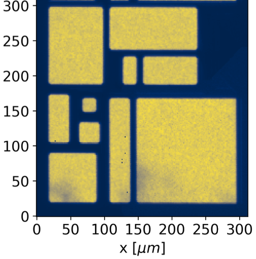
We have shown with prototype chips (upper left) that the dark count rates are independent of SPAD geometry and can drop to ~0.03 Hz/mm² active area
at liquid Xenon temperature (middle right) with an optimized SPAD technology, developed at IMS in Duisburg.
The spatial homogeneity of the SPADs is very good (upper right).
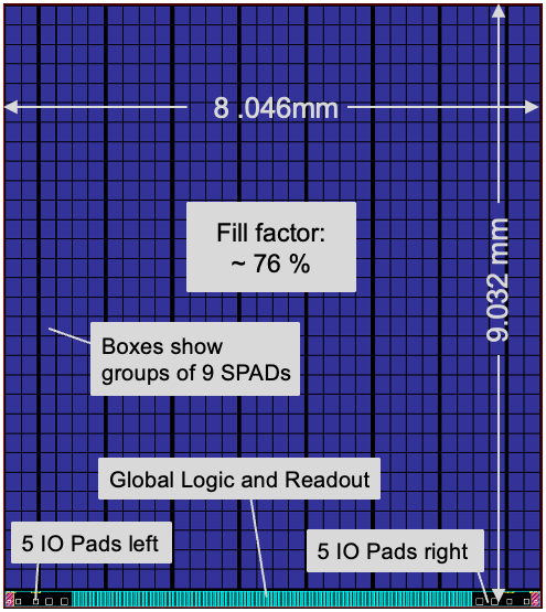
Our latest chip (lower left), which is currently in production, has a fill factor of 76% and a full readout which allows to daisy-chain many chips,
so that larger modules (middle right) require only very few signal cables.
The quantum efficiency of your chips is not yet sufficient for the UV light from liquid Xenon, but IMS is working on improving this.
Photo detection is also required in the NEXT experiment, which searches for neutrino-less double-beta decays
using pressurized gaseous Xenon. Our prototype chip for NEXT has a different readout architecture and is shown (bottom right).
Image Descriptions: (upper left) shows one of many pixels in our DARWIN prototype chip. Several SPAD geometries (with for instance different corner radii) have been used to study fill factor and dark count rate. (left second) shows the optical setup used the characterize the chips by shining < 1 single photon (per 'shot') onto well defined positions. (upper right) shows the fraction of detected photon 'shots' in 2 dimensions. The SPAD area has a very homogeneous sensitivity and the expected size. (right second) shows the dark count rate per SPAD area measured at varying (cold) temperatures. (left bottom) is the layout of the submitted latest DARWIN chip which included a full daisy chain digital readout. (right third) is an illustration of a possible DARWIN module with 16 chips. The right version uses the next chip iteration with wire-bond, the left the left side a potential design with larger chips and bump interconnect. (bottom right) is the layout of the submitted NEXT test chip.
Pixel in a test chip with different SPAD geometries.
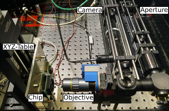
Optical test setup. A laser spot is focussed on the chip which can be moved with um precision.
Layout of the latest DARWIN Chip.
Position dependent single photon efficiency of a test pixel.
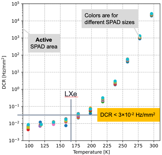
Dark count rates measured at low temperatures.
Concepts for larger detection modules. Due to their integrated readout, multiple chips can be daisy-chained.
Layout of the prototype chip for the upgrade of the NEXT experiment.
Project Description: We are investigating other applications of tailor-made chips for the detection of single photons and welcome potential 'users' to contact us to discuss their application. Some ongoing activities are:
- We have designed two chips with a rather simple X-Y-readout architecture: When a SPAD is hit, the row and the column are output as digital values. This allows to measure the arrival time of the photon with <1 ns precision. This simple concept only works for single hits, so that the chips can only be used for low photon rates, but that is often automatically the case when single photon detection is required. In case of multiple hits, the chip outputs an error flag so that no false information is recorded. This chip is intended for fluorescence lifetime imaging and will be used for electron microscopy.
- The technology offers the potential to measure ionizing particles by placing a scintillating material on top of the SPAD. We want to investigate this approach in cooperation with KIT. In a research project for the KATRIN experiment, we want to deposit tiny scintillator 'walls' in a square pattern. SPADs are only located under the 'walls', the electronics to process the SPAD signals is in-between. This leads to a very particular SPAD layout as shown in the layout (lower left).
- SPADs can deliver the arrival time of the photon with time resolutions well below a nanosecond, which corresponds to a flight distance of the photon of <30 cm. This offers the possibility to construct 3D cameras using the time-of-flight approach where the scene is illuminated with a very short laser flash and the arrival times of the photons are measured. A 'flash' camera does this in parallel in all pixels. Constructing a high resolution time measurement circuit with only few transistors in every pixel is an interesting design challenge. We have developed such a 'Time-to-Digital-Converter' (TDC) and build our flash camera chip BTDC (burst TDC) with 100×174 pixels. This chip is currently under characterization.
- The SPADs (and SiPMs) need a bias voltage of several 10 V to generate the necessary internal field for charge multiplication. It is often desirable to fine-control this voltage (affecting very much the SPAD gain) for each SPAD / SiPM so that a larger number of 'high voltage' power supplies is needed in the actual application. We want to investigate the possibility to generate these voltages in special chips to make systems more compact. A first prototype has been submitted recently.
Image Descriptions: Micro photograph (upper left) shows a small chip with 32×32 pixels (subdivided into 4 quadrants) implementing a fast XY-readout which provides a time information for every detected photon. It can measure several 10 million photons per second. (middle left) shows SPADs with rounded geometries which can be used to measure photon multiplicities in optical fibers. (top right) is a submitted experimental chip to investigate the possibility to produce the SPAD bias voltage of ~30 V on-chip, so that an external power supply is avoided. Micro photograph (bottom right) shows a large chip with 100×174 pixels which contains a precise TDC in every pixel. It may be used for time-of-flight measurements. The layout (lower left) shows a small part of a chip with a very special SPAD geometry (blue) for a project with KIT.
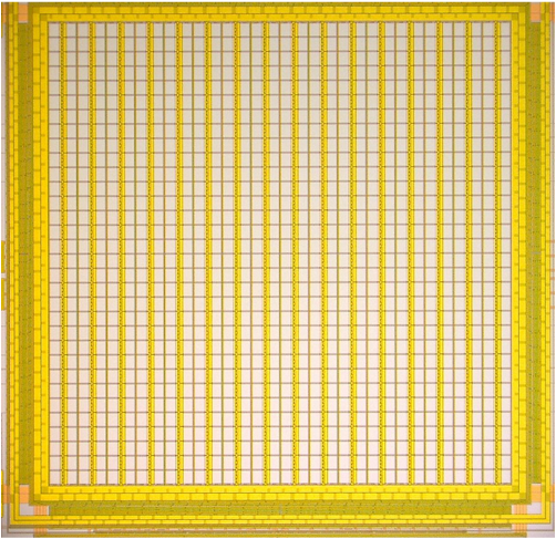
Photo sensor chip implementing a fast XY readout.
Various round SPAD structures.
Special SPAD geometry for the KATRIN project (@ KIT).
Chip for the generation of SPAD bias voltages of ~30 V.
Chip for Time-Of-Flight Measurements
Background: Synchrotron radiation is a very intense and focussed beam of X-rays which is produced by specialized accelerators. The radiation can be used for fundamental research, but also for 'routine' measurements in material science, biology etc. There are quite a few such machines available in Europe (see for instance the LEAPS initiative) and even more world-wide. In order to broaden the range of applications, the ESRF in Grenoble, one of the first machines in Europe, has increased the beam energy significantly so that the 'Extremely Brilliant Source' EBS can now deliver X-rays with energies up to 100 keV. Because of their high energy, such X-rays are very penetrating and commercially available 2D-cameras are not able to detect them with satisfying efficiency.
Project Description:
The ESRF has therefore initiated and financed an R&D project with the goal to develop and demonstrate a concept for a 2D X-ray camera
which can detect X-rays with high energies and very high intensities (up to 109 X-rays per second per mm²) and
which is fast enough to cope with the time structure of the photon 'bursts'.
The XIDer 'X-ray Integrating Detector' uses a novel charge-pumping scheme to remove charges quickly from the sensor in
order to reach high intensities and linearity at the same time. The incoming charge packets are digitized continuously and added up
in the digital domain ('digital integration' concept). Each pixel has an on-chip memory where data can be stored or accumulated for later
readout. A 'histogram mode' allows for data reduction. The various processing options are controlled by a flexible 'telegram' protocol.
In order to detect the high-energy X-rays, materials with a high atomic number must be used. The most promising candidate is 'Cadmium-Zinc-Telluride' (CZT),
but we are investigating other materials like CdTe or GaAs as well.
Our Heidelberg group is fully responsible for the chip design, for readout and the assembly of prototypes. The available test chips (with just 4×4 pixels so far)
are fully functional and the collaboration has successfully measured X-rays at the beam at ESRF.
Similar as ESRF, the 'Diamond Light Source' DLS and
STFC in the UK are working on a 2D detector in their DynamiX project.
The two projects are presently merging forces, forming XYDyn. A first common chip with 16×16 pixels of 110 × 110 μm²
implementing both circuit versions has already been produced and is presently being tested.
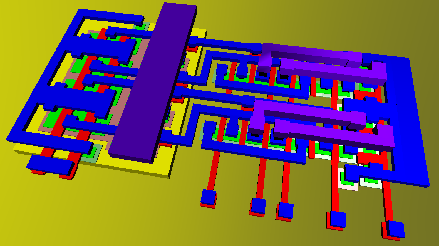
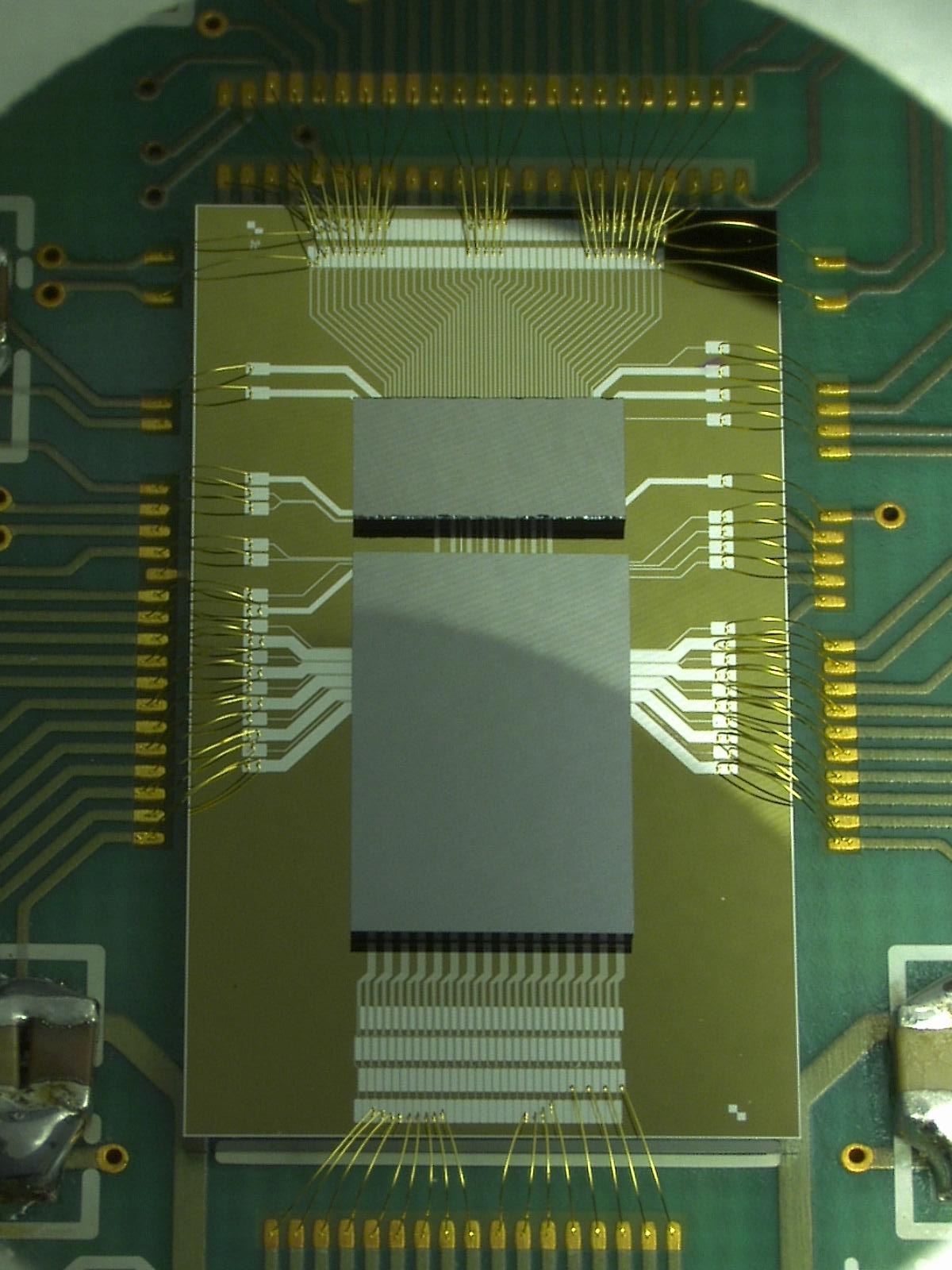
Image Descriptions: (upper left) shows a photograph of a CZT sensor flip-chip mounted to a small test chip. The wire bond pads are at only two chip edges to leave space for the sensor. The 4×4 usable pixels are in the small overlap region. (middle left) shows the layout of the XIDer part of the common test chip. All IO pads had to be squeezed into two rows in the small area in the upper right part. The wire-bonding of this chip is therefore quite challenging. The photograph (upper right) shows the successful bonding in Heidelberg by Ch. Kreidl in two levels. Micro photograph (lower right) shows the fabricated (rotated) chip. The layout (lower left) shows a custom designed memory of 256×16 cells which has an area of only 81.1 × 43.1 μm² in the 65 nm CMOS technology used.
Assembly of a XIDer prototype chip with a CZT sensor.
Layout of a matrix with 16x16 pixels in the latest test chip.
Layout of the memory for one XIDer pixel.
Two level bonding to the upper right corner of the latest test chip.
Micro photograph of the larger text chip (XYDer part).
Background: Modern PET scanners used for medical imaging (see also the PET module section) use a large number of small photo detectors, often SiPMs, to measure the light generated in scintillating crystals. This allows to determine the impact position of the 511 keV gamma pairs from positron annihilation with high precision in order to obtain a 3D image with high resolution. The signal of each SiPM must be amplified, hits must be detected, the amplitude must be measured and the time of arrival must be measured with a precision of some nanoseconds for coincidence determination, but much better if the 'Time-Of-Flight' method shall be used. Due to the large number of channels, it is not feasible to bring out all signals to external electronics with cables, so that the data processing functionality must be done very close to the SiPMs.
Project Description: We are developing since many years special purpose microchips which can process signals if ~32 SiPM channels each. The PETA (PET-Energy-Time-Amplifier) have a size of 5×5 mm² and contain for each channel
- a fast low noise amplifier,
- a fast discriminator with programmable threshold to trigger on hits,
- a charge integrator which is started by the discriminator an accumulates all incoming signals for a programmable duration,
- a ~9 Bit ADC which converts the integrated charge to a binary value,
- a timing circuit which measures the hit with a resolution of 20 ps (!),
- a 'neighbor logic' which allows to force-trigger arbitrary other ADCs so that the light created in neighboring crystals is measured even if that channel did not self-trigger. The neighbor information can be used to improve spatial resolution.
We are presently working on an improvement of the readout which is required to bring the hit data from the chips to the data acquisition system. Instead of connecting each chip to a control and readout FPGA, as it is common practice, data is sent from chip to chip so that no further circuitry is needed. As a side effect, data is sorted in time so that the subsequent processing is eased a lot and a data reduction inside of the PET scanner is feasible (discard gammas with no coincident partner, sum up energies and discard Compton scatter events, ...). As a further system improvement, we are investigating the possibility to power the chips in a serial topology to reduce the supply currents and the induced voltage drops.
Image Descriptions: (top left) shows the PETA8 chip with a size of 5×5 mm² and 99 bumps in a pitch of 0.5 mm. A zoomed micro photograph of the lower left corner is shown in (top right). (bottom left) shows the USB3 based test setup which we use to characterize PETA (and other chips). The 'device under test' is place on an exchangeable PCB on the left, another PCB with SIPMs can be connected to the right connector. (bottom right) shows an illustration of a 'tree' interconnect topology of 64 chips, where data of groups of 3 chips is merged successively until all data leaves the last chip at the red arrow.
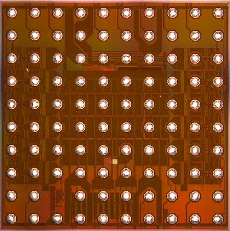
PETA chip of 5×5mm² size with solder balls. One ball has been left out on purpose to fix the chip orientation.
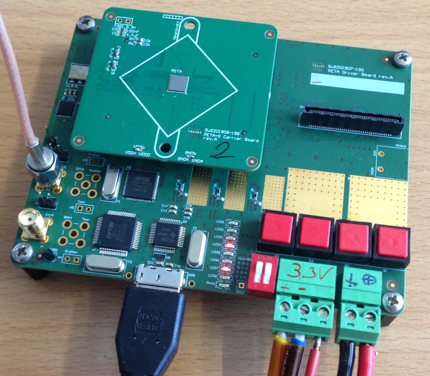
USB test setup used to characterize PETA and many other chips in the group.)
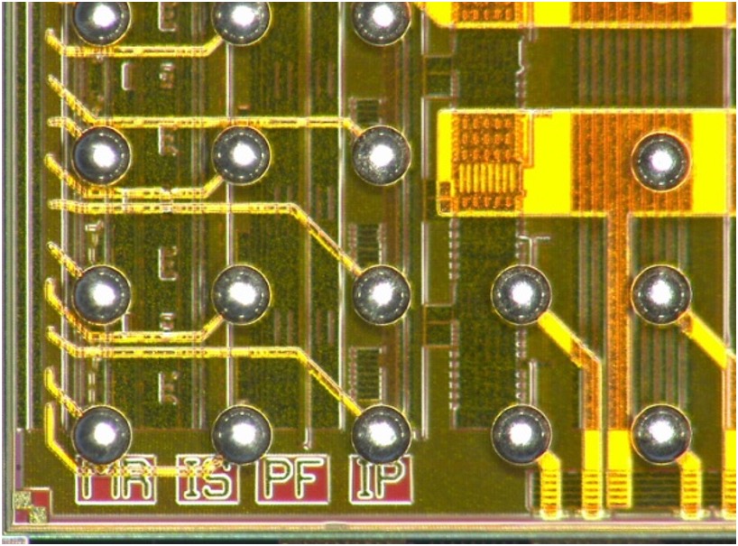
Detail of lower left corner with designer initials 'Michael Ritzert, Ilaria Sacco, Peter Fischer, Ivan Peric'.)
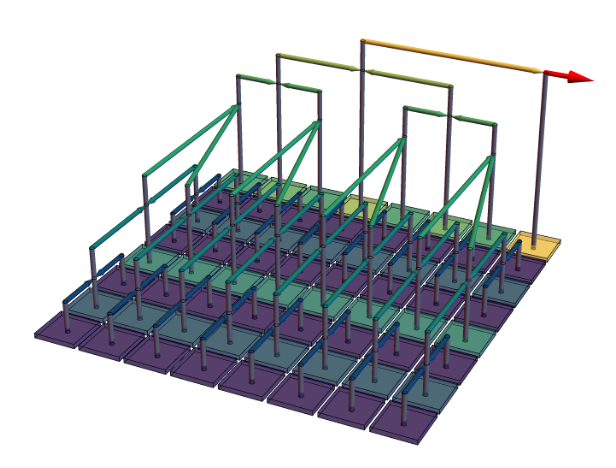
The latest PETA chips can send data from one chip to another. The picture illustrates a possible interconnection topology.
Background: Large PET scanners for clinical patients and smaller scanners for 'brain-only' imaging are available commercially, and there are 'small-animal' scanners on the market for research. However, there are still new ideas or special needs coming up, so that some groups with enough hardware competence want to design own special purpose PET rings. While two main components of typical designs - the crystals and the SiPM photo sensors - are available commercially by several vendors, the third component - the readout ASIC - is more difficult to find. Therefore, several groups cooperate with us using the PETA chip developed in our group.
Project Description:
The SAFIR project at ETH Zürich has build a small animal scanner which can do PET imaging
at very high does rates (up to 500 MBq applied dose) so that PET images can be recorded every few seconds. This allows the
observation of dynamic processes, like the time evolution of the distribution of a tracer after injection.
The scanner has been fully designed, constructed and operated by the ETHZ group, using PETA chips and some control
firmware from Heidelberg. The ring is very compact and designed in a way that it can be operated inside of a MRI scanner, so that
high resolution MRI images and functional PET images can be taken simultaneously and then be superimposed.
A particularity of SAFIR is the use of switch-mode DC-DC converters operating with air coils (to avoid magnetic saturation in the static B-field
of the MRT) constructed in a clever way that the dynamic magnetic fields do not disturb MRI imaging.
A follow-up project at ETHZ is the brain PET PETITION
which will be used in proton treatments at PSI.
A third research application of PETA chips is a scanner developed by the group of Craig Levin in Stanford.
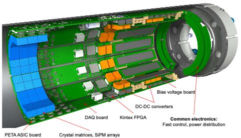
Image Descriptions: (upper left) shows a 3D illustration of the SAFIR ring. The crystals with SIPMs and PETA ASICs are the blue boxes on the left. This ring is composed of modules with 2 wrapped LYSO crystals and 4 chips, as shown (upper right). An image of a rat and the obtained state-of-the art coincidence resolving time CRT of 204 ps are shown (bottom left). All pictures are from ETHZ.
3D view of the SAFIR PET scanner constructed at ETH Zürich. (Drawing by ETHZ)
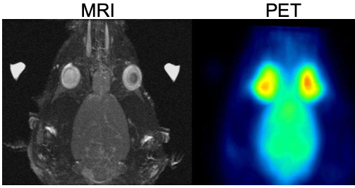
MRI and PET images of a rat taken by the SAFIR ring at ETHZ. (Picture by ETHZ)
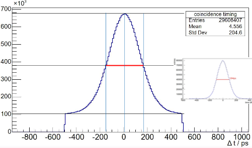
Time resolution ('coincidence resolving time') achieved in the final system. (Picture by ETHZ)
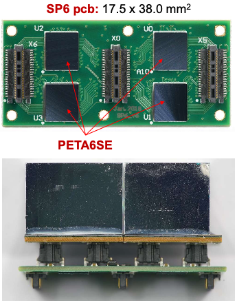
Modules used in SAFIR. A PCB contains 4 PETA chips and connectors to connect two small boards with SiPMs and LYSO crystal arrays. (Design and picture by ETHZ)
Background: With the goal to speed up computations and/or to make them more energy efficient, several groups, like AG Pernice at KIP, investigate the possibilities of optical computing. In one approach, an external laser pulse is first coupled into a waveguide on the surface of an (optical) microchip. The light is then equally distributed to a number N of waveguides, so that they all receive an amplitude I0. In each waveguide a 'modulator' is then used to lower the pulse intensity so that the level in the i-th waveguide is Ii = ai I0. The N modulators are controlled electrically with fast pulses. The multiple attenuated light pulses are then coupled into an output waveguide. The coupling strength of each contribution Ii can be adjusted in some way with weight factor wi. The intensity in the 1st output fiber is therefore O1 = Σi=1…N wi Ii, i.e. the sum over all contributions. This corresponds mathematically to a scalar product. If multiple output waveguides Ok (k=1…M) are used (and many more weights are available), M outputs can be computed simultaneously: Ok = Σi=1…N wki Ii for k=1…M. This is a matrix product.
Project Description:
While the actual computation is done optically, the values to use must normally be provided by a digital system.
In particular, the modulators must be controlled and the weights must be set in some way.
Prototype structures can use single channel commercial equipment, but the anticipated multi-channel systems require
solutions with many channels in a compact chip.
We have therefore developed a fast Digital Analog Converter (DAC) circuit which converts an 8 bit digital value
to a steering voltage for an optical modulator.
The circuit is not back from fabrication yet, but we hope that it can convert more than 500.000.000 values per second.
In order to steer multiple modulators in parallel, the actual chip (left) contains 8 channels.
A second chip is used to control the weights. This can be much slower, as they are typically changed less frequently
in applications like image processing or machine learning.
A third chip has a bit different scope: It can be used to measure low photon intensities in optical fibers (lower right).
It consists of an array of 9×9 small SPAD photo sensing elements which are read out at high speed, counting the
number of hit SPADs in each 'frame'. This chip has actually been designed by students of the VLSI design lecture.
Image Descriptions: (left) shows the 8 channel DAC chip with a size of 1.5×3mm². The 8 identical channels are clearly visible. They contain a significant amount of digital circuitry to set many control bits and to provide digital information to the actual DAC at high speed for testing. The many bonding pads left and right are mainly for power to guarantee stable operation at high speed. (upper right) is the chip for weight adjustment. It has a number of multiplexed outputs on the right side and a common central digital block. (bottom right) shows the chip with the SPAD array (on the right side). The chip leaves generous space between the SPADs and the IO pads to simplify the mounting of the optical fiber on top.
Fast DAC chip with 8 channels for optical computing.
Chip designed to drive laser diodes.
Single Photon detection chip for photon multiplicity measurement. An array of SPAD sensors is located at the right.
Background:
One of the big detectors at the accelerator facility FAIR is
CBM ('Compressed Baryonic Matter'). This experiment uses several different
sub-detectors to track and identify particles which will be created in heavy ion collisions.
One of the sub-detectors is the over 100 m² sized 'Transition Radiation Detector'
TRD which will be used to distinguish pions from electrons.
It consists of several layers of material in which the traversing particles produce a varying number of X-rays, depending on their velocity.
These are then detected in a gas-filled 'Multi Wire Proportional Counter' where high electric fields
in the vicinity of thin wires amplify the charges generated by the X-rays in the gas.
The 2D position of the avalanches is detected by the charge influenced from the gas avalanches on pads of some cm² size
on the backplane of the TRD. Because electrons are lighter than pions, they are often faster and produce more
transition radiation so that the observed charge is higher.
The charges induced on the pads of several 1000 electrons must be amplified, detected, digitized and sent to the
data acquisition system of CBM with a special purpose microchip.
Project Description:
We are developing the SPADIC chip ('Self Triggered Pulse Amplification and Digitization ASIC') for the readout of the TRD of CBM.
SPADIC has 32 channels on a chip area of 5×5 mm² and is packaged in a compact BGA case.
Each channel contains a low noise charge amplifier / shaper with a peaking time of ≈ 200 ns followed by
a free running 9 bit Analog to Digital Converter (ADC).
The data stream can then be filtered with a programmable digital Infinite Impulse Response filter (IIR).
A versatile digital hit logic detects hits in the resulting data stream and passes a selectable set of pulse samples to the readout part
which collects the hits (including time information) and sends them off-chip through two serial links, following the CBM specific
protocol. The time order of the hits is preserved to simplify further online processing.
Many buffer memories are available to de-randomize the data.
Several iterations of SPADIC have already been produced, with some setbacks.
For instance, the initial readout protocol of CBM ('CBMNet') has been replaced by a version using the E-link protocol from CERN, so that
the complex digital data interface had to be exchanged (new code provided by AGH in Krakow). In one chip production, the multiple memory blocks
were accidentally not filled in by the vendor, so that large parts of the design could not be checked. Because the specially developed and
fabricated packages had to be used before their expiration date, the partially tested design was used for a larger production.
It turned out that the ADC design was performing well on many channels, but a (too) large number of ADCs had unsatisfactory performance.
The yield of well-working chips is therefore too low and we are presently investigating how to solve that issue.
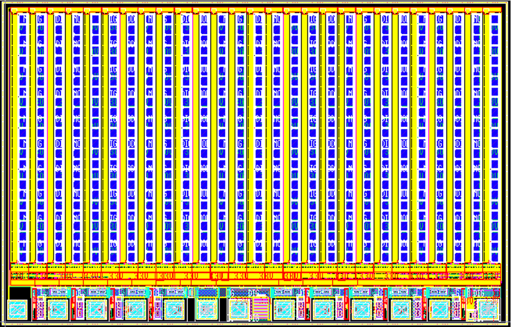
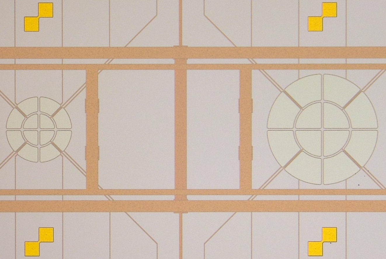
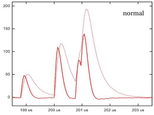
Image Descriptions: The layout (left top) shows a 5×5 mm² SPADIC chip. The 32 amplifiers are on the left, followed by the ADCs. The large part on the right are the digital filters and the readout logic. The black rectangles are free spaces for memories, which are later added by the vendor. (left middle) is a micro photograph of a chip wire-bonded in Heidelberg to a test PCB. Due to the high number of connections, the PCB design using 'standard' design rules is quite challenging. The simulation (left bottom) shows the action of the digital IIR filter. The width of the light-red pulses from the preamplifier can be compressed (red) to increase the rate capability. Photograph (right top) shows a test setup which is used to verify chips in their BGA package. The board only receives power and sends data to the CBM links via one cable on the right side. The measurement (right middle) shows 32 pulses from the amplifier/shaper digitized by the ADC, demonstrating its correct function. (right bottom) is a nice photograph (by GSI) of a silicon wafer from a production run organized by GSI containing, among others, SPADIC chips.
Layout of a SPADIC chip.
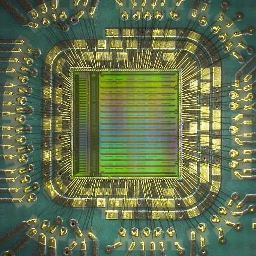
Photograph of a SPADIC chip bonded to a custom-made PCB.
Simulation of the digital IIR filter implemented in SPADIC used to shorten long detector pulses.
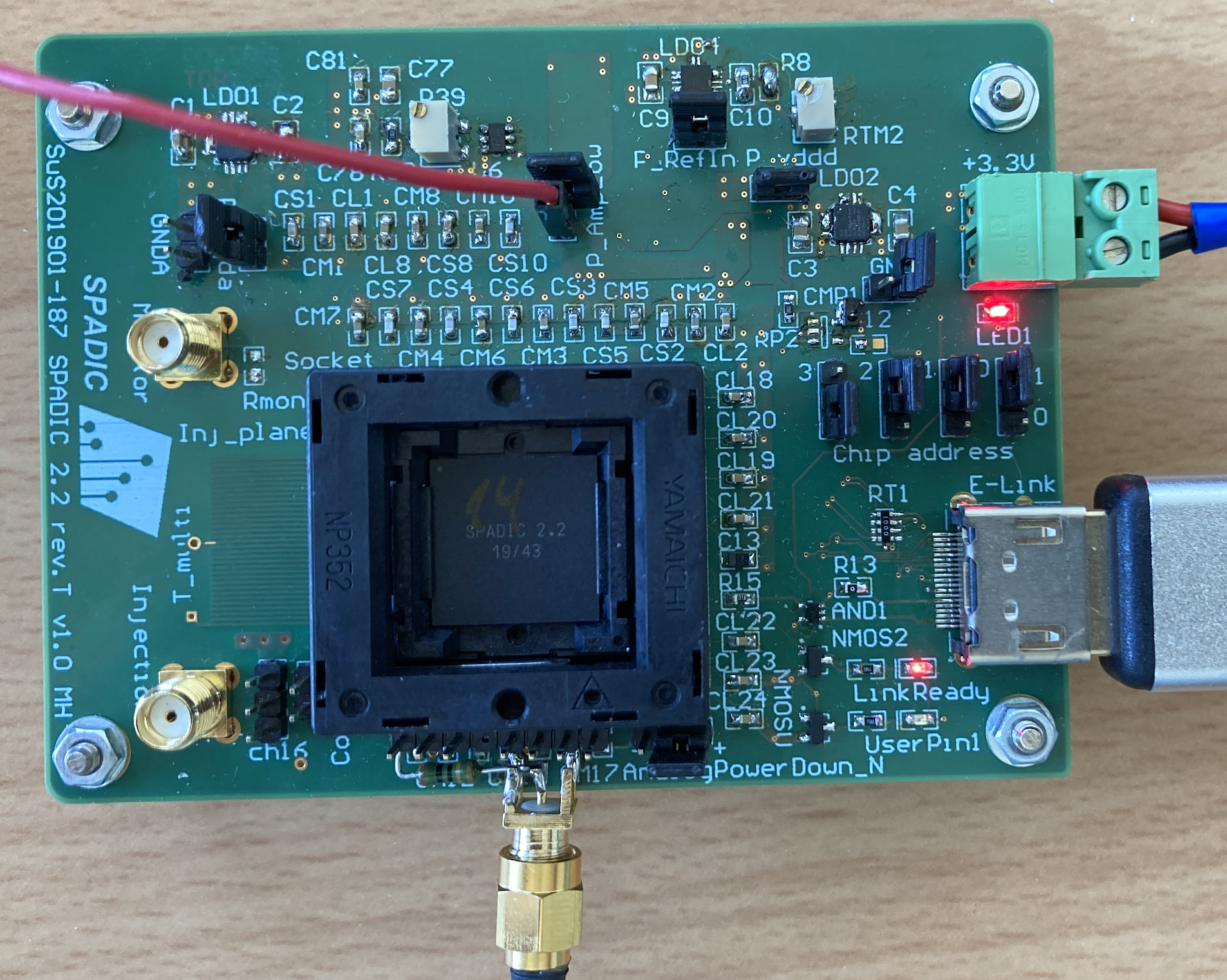
PCB setup to series-test packaged chips.
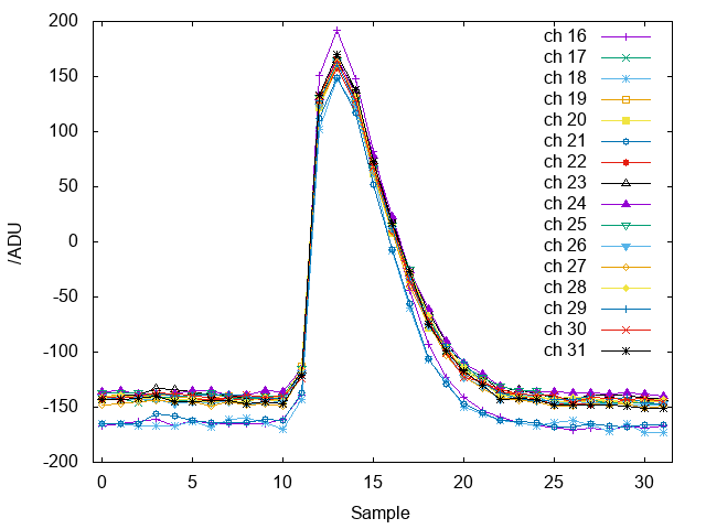
Measured ADC pulses.
SPADIC Chips (and others) on a wafer production organized by GSI (Photograph by GSI).
Background:
PET scanners typically consist of a cylindrical arrangement of detection modules around the patient.
The modules must detect the pairs of gamma particles emitted back-to-back in the positron annihilation process.
Due to their high energy of 511 keV (the rest mass of electron/positron), these gammas are very penetrating
(which in fact allows them to traverse the patient body) and hard to detect. One common approach is to absorb them
with a good efficiency in crystals made from materials with very high atomic number, like LYSO
(containing Lutetium and Yttrium). Typical thicknesses are 10-20 mm.
The energy deposited in the crystal generates optical scintillation photons which are detected by photo sensors
located at the backside of the crystals.
In order to determine the precise impact position of a gamma, the scintillator crystals are often
segmented into small 'columns' of some millimeter lateral dimension. In modern scanners, ~1000 photons
leaving the crystal columns at the backside are detected by silicon based photo detectors, the 'SiPMs'. Unfortunately,
the SiPMs only deliver very small electrical signals when hit by the photons and an amplifier is required for each SiPM.
Due to the high number of crystal columns, and thus a high number of SiPM elements (in the so called 1:1 arrangement
discussed here), many electronics channels are required. In modern scanners, specialized readout ASICs (see next section)
are used.
Bringing all elements together is a big challenge: The Crystals must be optically coupled to the SiPMs, these must be electrically
connected to the ASICs. The ASICs require significant supply current, produce heat and must be cooled efficiently to avoid
overheating of the module and of the SiPMs which degrade in performance when warm. Also, the chips must be steered and
the hit data must be read out.
Project Description: The module shown on the right has been developed by our group within the EU Project 'Hyperimage'. It is centered around a 3.3×3.2 cm² ceramic carrier board specified by us and manufactured by project partner company MSE. The ceramic contains 10 internal routing layers to interconnect the SiPMs at the top side and 4 ASICs and a connector at the bottom side. In addition it contains an internal water channel (!) for a very efficient cooling of the ASICs. The manufactured modules are fully functional and demonstrate state-of-the art PET performance in terms of spatial resolution (2.5 mm pitch) as well as (prototype) time resolution (CRT of 232 ps).
Image Descriptions: (top right) shows the top side of the ceramic with 2×6 large SiPM chips specified by us and manufactured by project partner FBK . Each SiPM contains 12 sensing elements of ≈2.5×2.5 mm² each. The segmented crystal array is later glued with a transparent glue to the SiPMs by our team. The SiPMs are electrically connected at the edges to the ceramic with tiny wire bonds, performed by our group. (top left) shows the module with a glued crystal from the backside. The 4 PETA readout ASICs, developed in our group, are flip-chip mounted. Only few additional components (decoupling capacitors, temperature sensor) are required. One connector provides power, control and reads data. Also visible is an improvised connection for the water flow through the ceramic. (middle right) shows the flip-chip mounted PETA ASICs of ≈5×5 mm² size in more detail. (bottom left) is a lab setup to operate two modules back to back. The first time resolution measured with this setup is shown (bottom right).
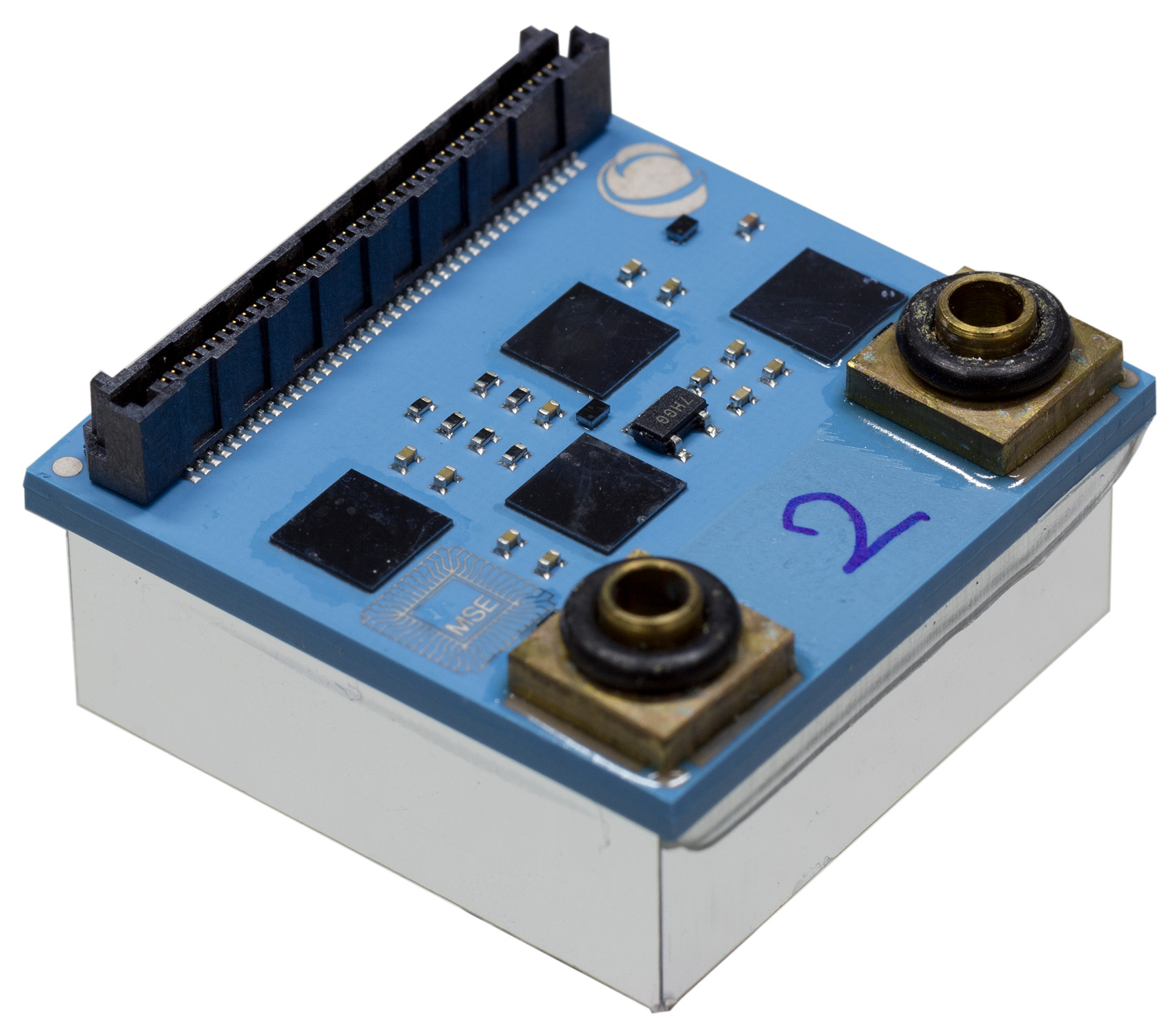
Complete gamma detection module. The (wrapped) LYSO crystal array is at the bottom.
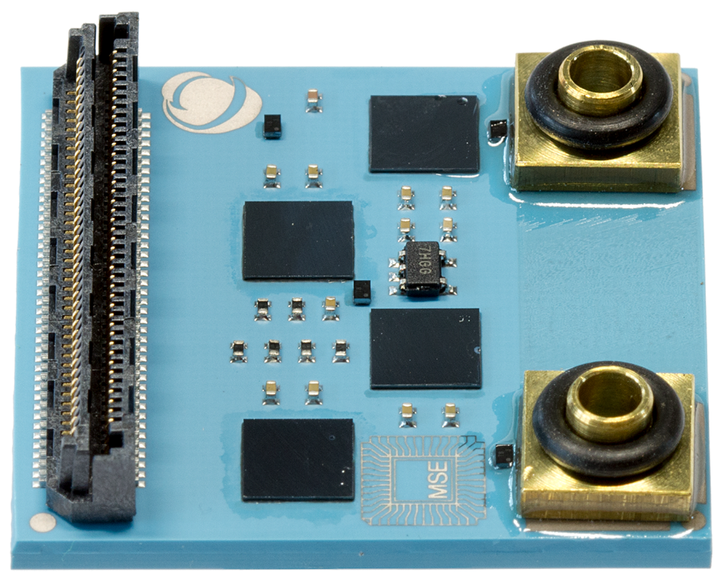
Top side of the ceramic board with mounted PETA chips.
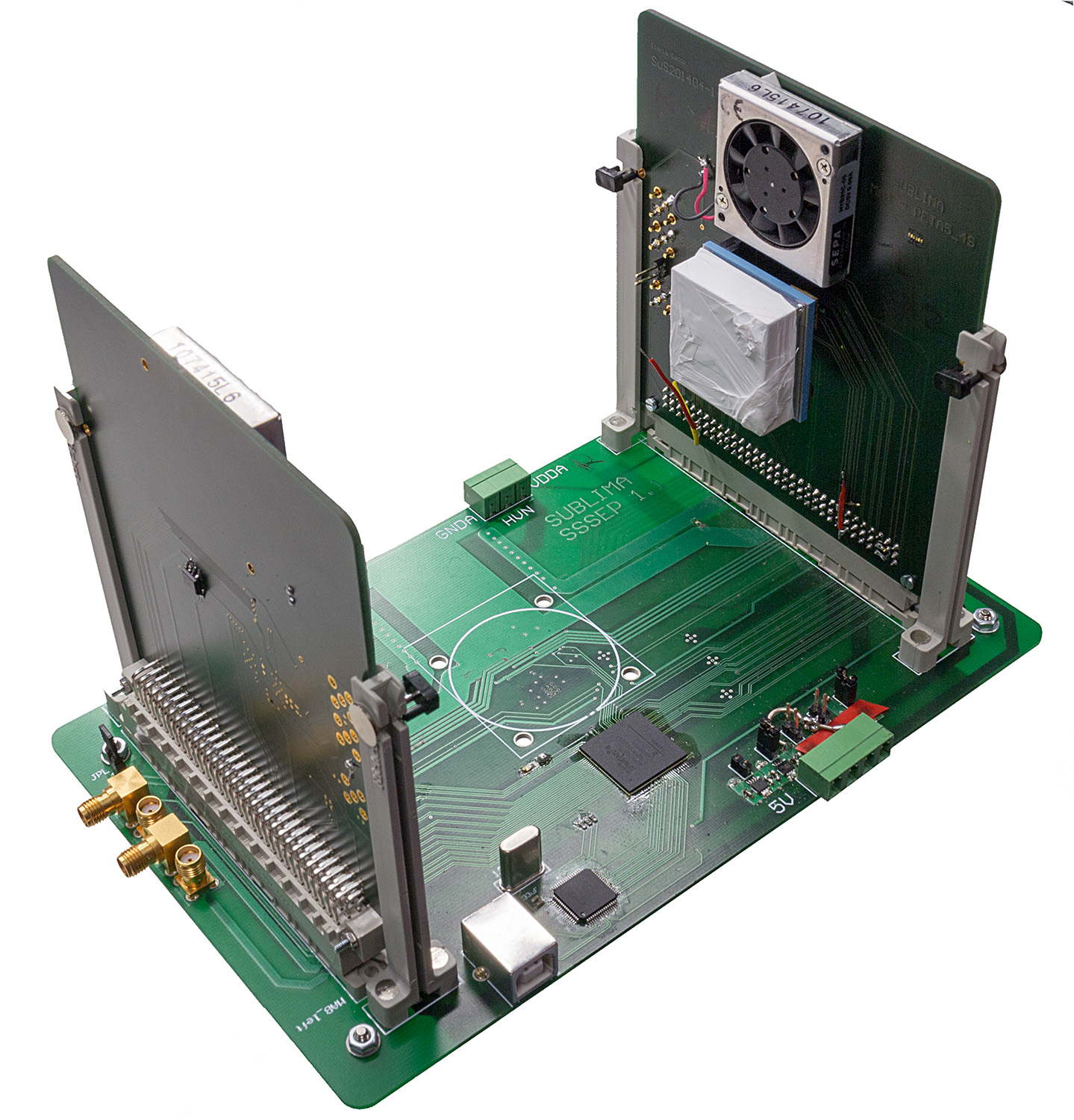
Readout system used to test PET imaging with 2 modules.
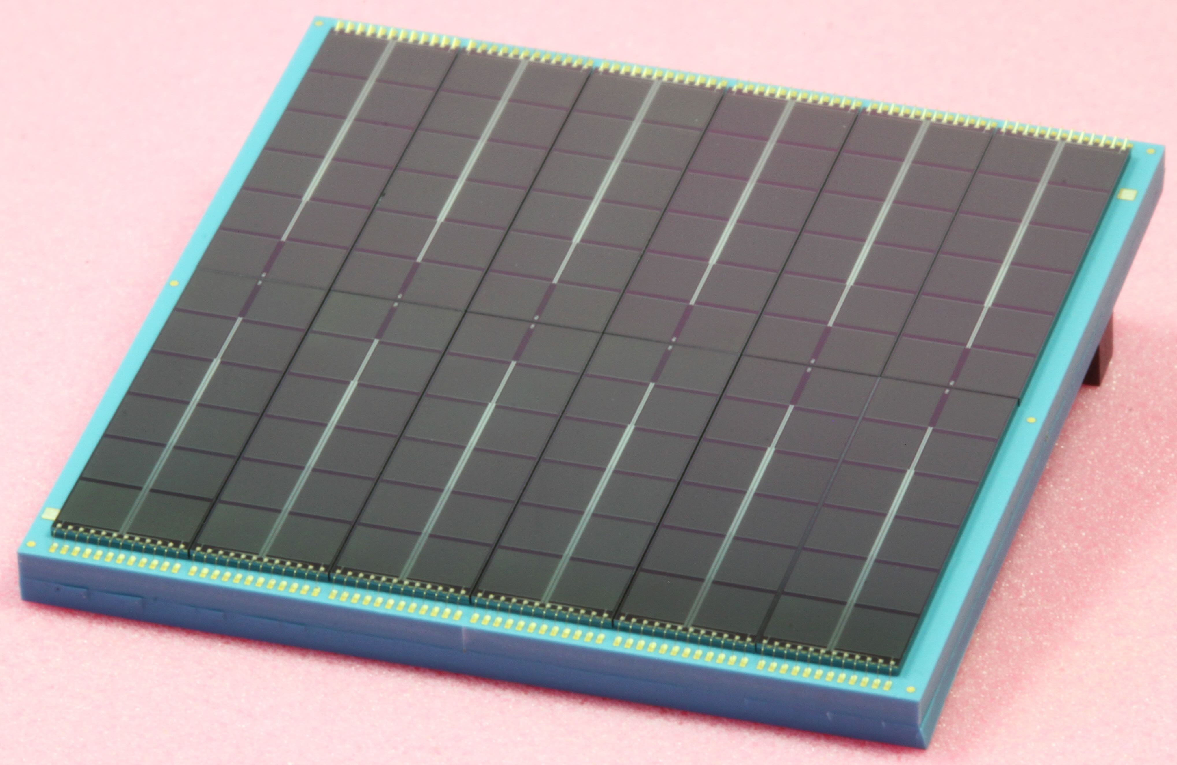
SiPM sensors on the bottom side.
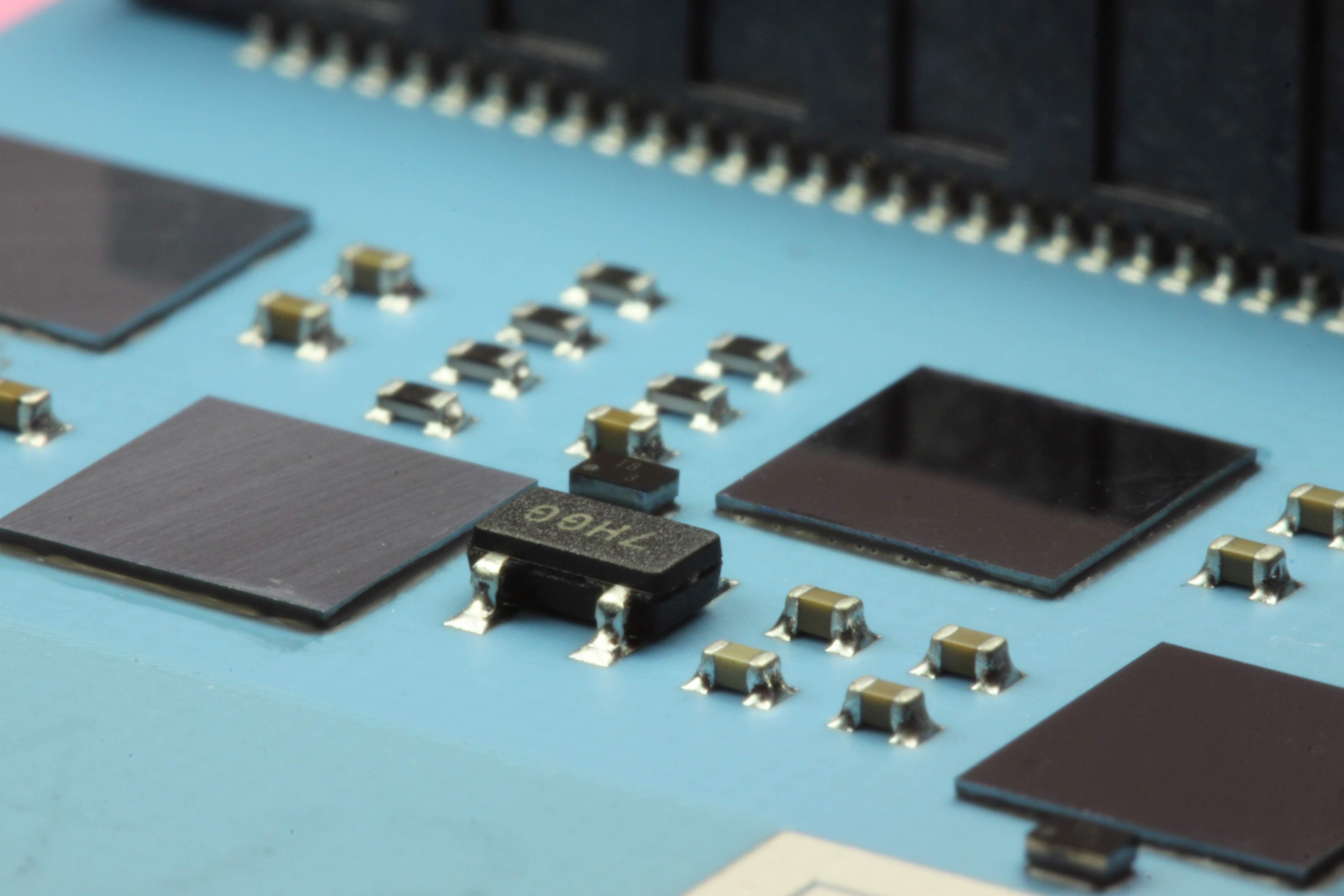
Detail of flip chip mounted PETA ASICs
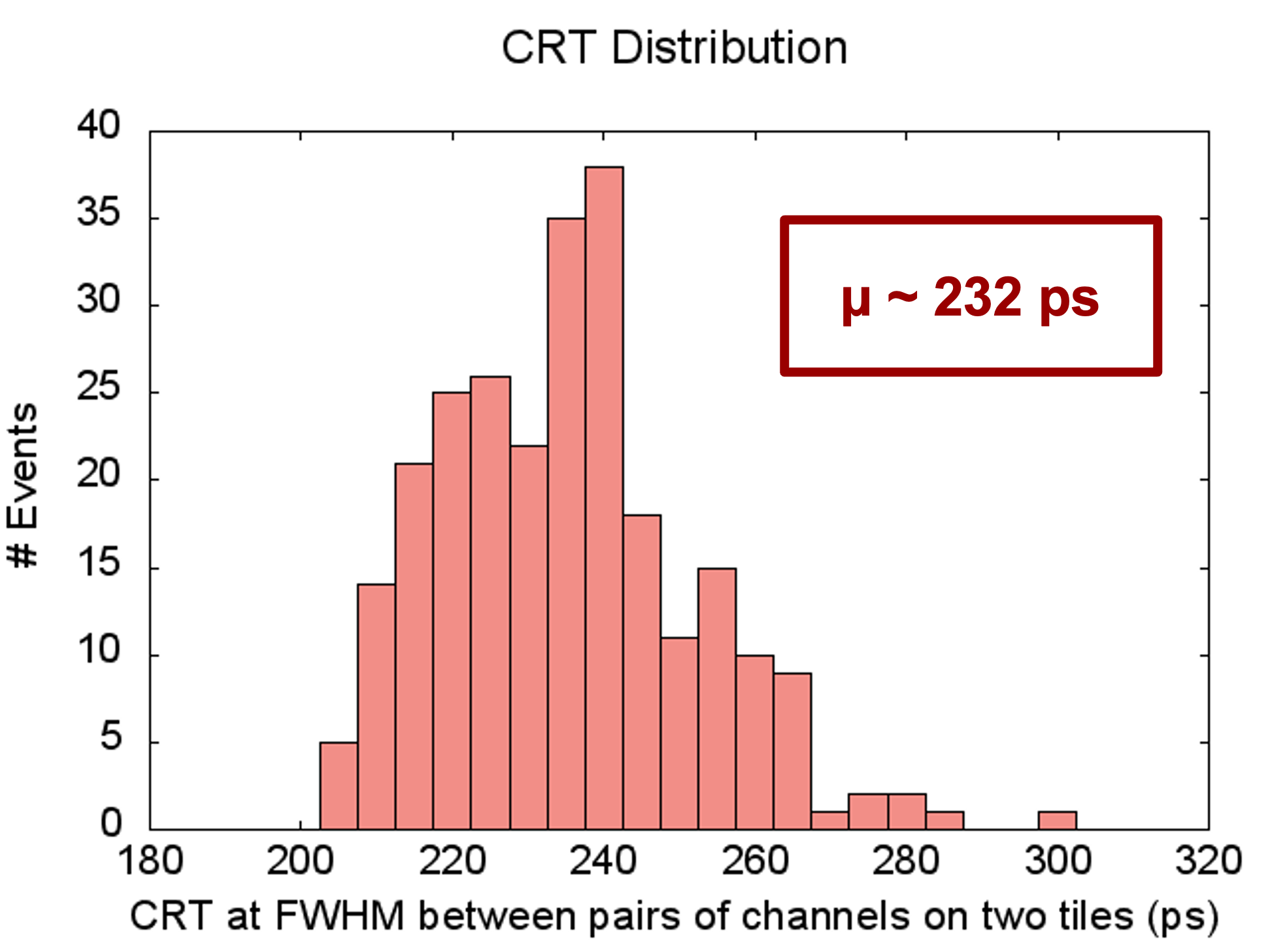
Coincidence resolving time measured in the prototype test system.
Background: The EuXFEL is a free electron laser facility which has been completed ~2018 in Hamburg. The machine produces very 'brilliant' X-ray pulses with a particular time structure: 10 times per second, up to ≈ 3000 X-ray flashes spaced in time by ≈ 200 ns are delivered in a 'pulse train'. At the time of construction, such fast pulses could not be resolved by available 2D imaging detectors and therefore EuXFEL initiated a R&D program with the goal to develop suited 2D 'camera' detectors with 1000×1000 pixels. A particularly challenging requirement is the low energy of the X-rays of below 1 keV (in some applications), so that the charge deposited in silicon detectors is very small such that low-noise - but still fast - electronics is required. Another challenge is the required dynamic range which should span from the safe detection of a single X-ray up to many 1000 in one pixel.
Project Description:
DSSC ('DEPFET Sensor with Signal Compression') is one of three projects initiated and funded by EuXFEL.
We addressed the 'low energy challenge' by proposing to use a rather novel type
of silicon detectors, the DEPFET ('Depleted Field Effect Transistor').
In each pixel, these silicon devices first collect the charges on an internal 'electrode' with very small capacitance and then
use this charge to modulate the current of an integrated transistor.
This current is then passed to pixelated readout chips which are flip-chip mounted to the larger DEPFET sensor.
By a clever shaping of the 'internal gate', the current is not a linear function of charge and a favorable signal
compression (requiring careful calibration....) is obtained.
Each chip pixel contains a special low noise 'trapezoidal' filter, a 8-9 bit ADC (depending on operation speed) and a digital memory
to store up to 800 samples during the burst (more circuitry did not fit in the pixel area of 229×204 μm²).
The collected data is sent off-chip serially 10 times per second in the gaps between the bursts.
A fancy triggering scheme allows to re-use memory cells during the burst if data can be discarded.
After a successful prototyping phase, difficulties occurred in the procurement of DEPFET sensors, so that we had to move
to another sensor type. To approach the desired noise performance, we decided to use small Silicon Drift Device ('MiniSDD') in each pixel
and had to modify the readout ASIC accordingly. Recently, DEPFET devices have become available and the latest modules
reach an impressive noise performance of only 10 electrons (equivalent noise charge, rms) at a speed of 1.1 MHz, see
for instance here.
Our main contributions to DSSC were ASIC design, the mechanical assembly of prototypes (bonding, flip-chip), readout systems,
intensive characterization of chips and sensors, and several components to the final data acquisition system.
For the ASIC design, several DSSC partners contributed important analogue building blocks (ADC, Filter, References, Pads,..).
Our group designed further blocks (like the RAM or precise DACs), developed the full digital part, did integration, assembly and
verification of the full-size chip and managed the fabrication process. The fabricated bumped chips were wafer-probed in
Heidelberg to pick the 'Known Good Dies' for module assembly.
On the DAQ side, we developed the 'IOB' board which receives the serial data from 16 ASICs and passes it though 4 fast serial 'aurora' links to
the 'PPT' data concentrator board, also developed in Heidelberg.
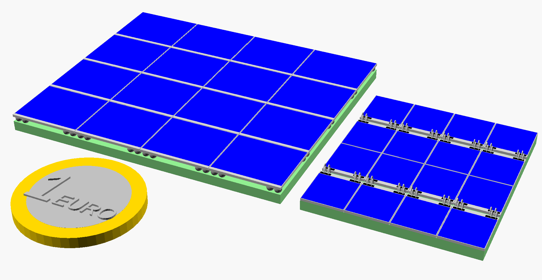
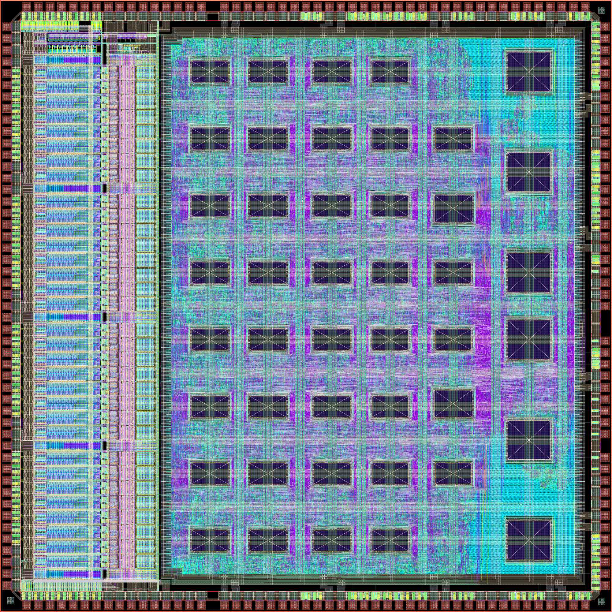
Image Descriptions: (left top) is the layout of one pixel in the readout ASIC. The main components are the charge amplifier / filter on the left, the ADC on the right an the memory on top. A small digital section in the middle coordinates the various blocks and contains configurations bits. (left middle) shows the full chip with 64×64 pixels and a small periphery part with input/output pads. The photograph (left bottom) shows a fabricated chip with solder bumps in size comparison to a 1 € coin. The balls are better visible in the nice magnified photograph (right bottom). The completed DSSC camera, as it is now installed at EuXFEL, is shows (right top). Four quadrants can be moved in x/y to leave space for the primary beam in the middle. Each module contains 4 large DEPFET / MiniSDD sensors with 8 chips on the backside. The whole camera is located in a vacuum vessel which is attached to the beamline, for instance at SCS. The vacuum operation makes it challenging to cool all electronics components with a liquid cooling system. All electrical connections for power and data handling and the tubes for cooling are located at the backside, not visible in the picture.
Circuit elements in one pixel of 229×204 μm²
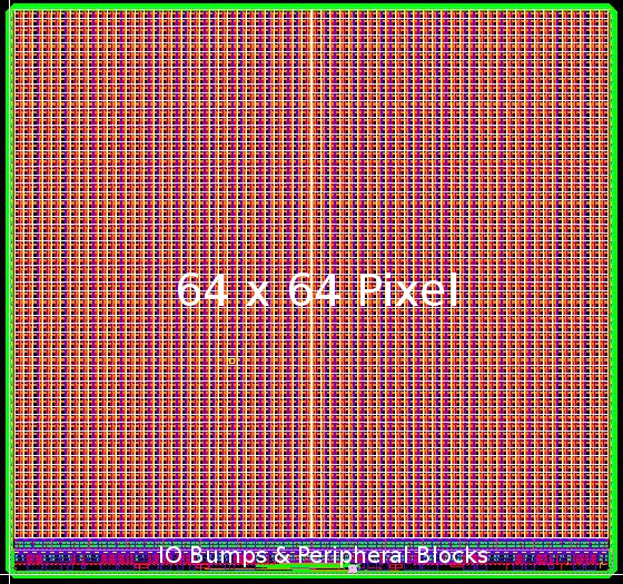
Layout of the DSSC readout chip
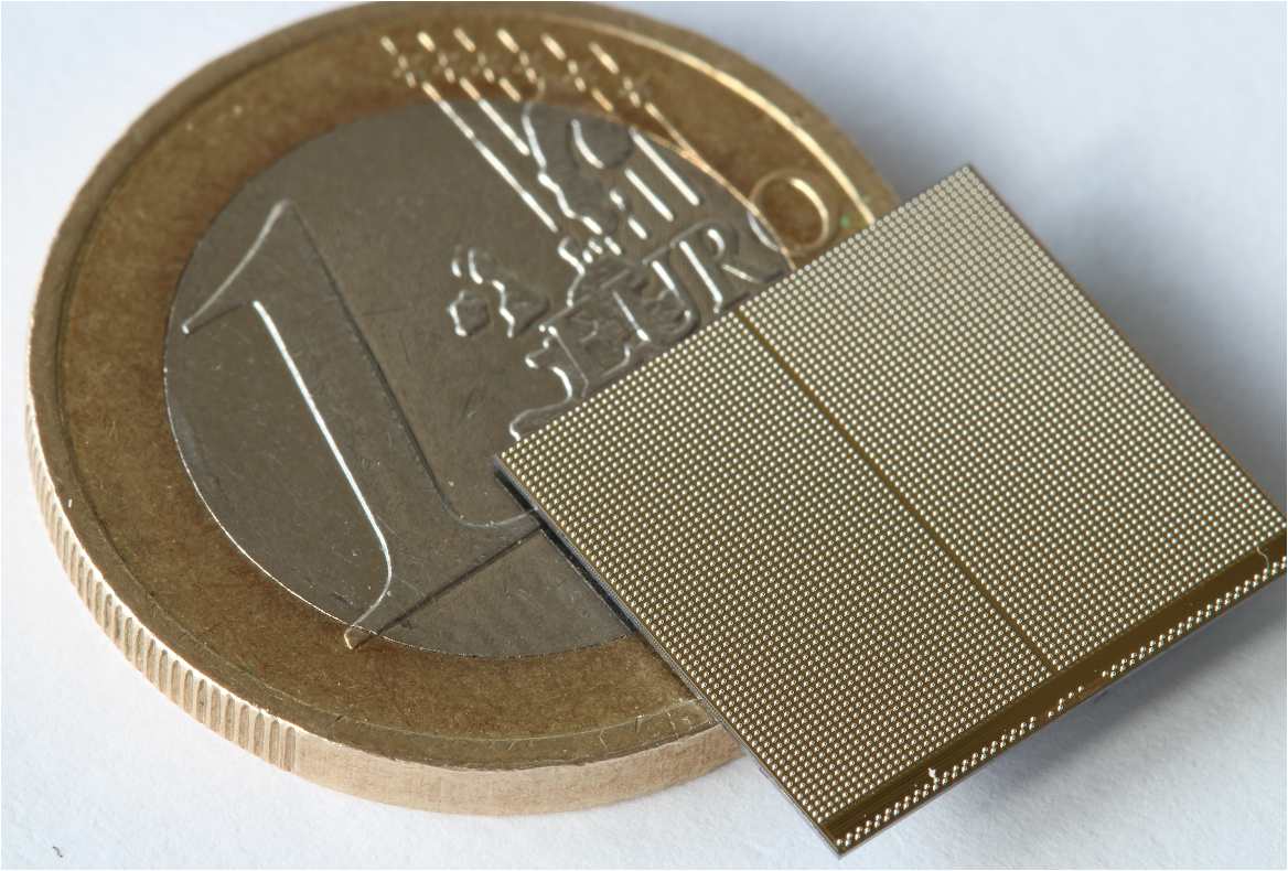
DSSC readout chip with bumps, compared to coin.
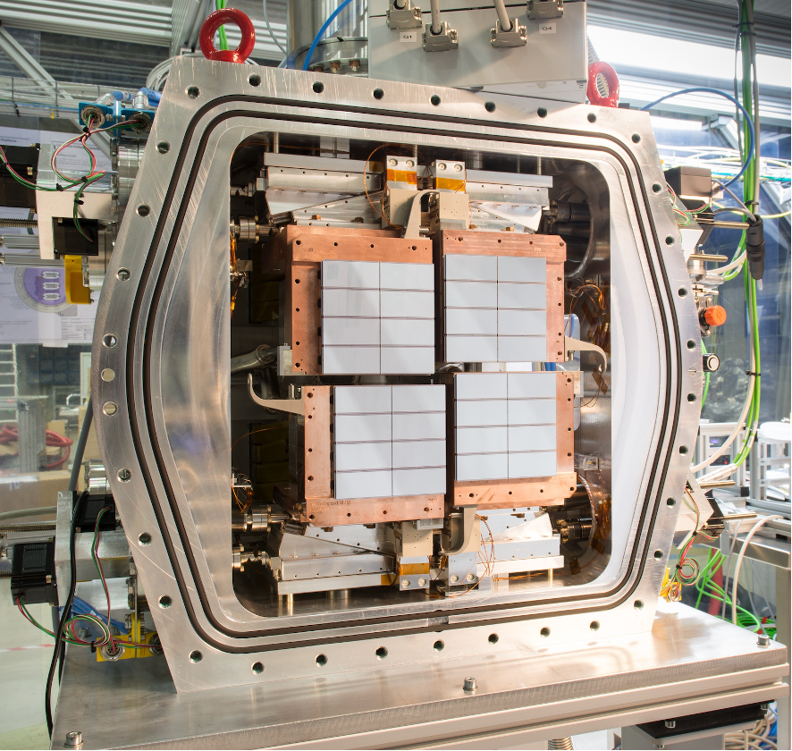
The completed DSSC Camera in its vacuum vessel at the Eu-XFEL. The active area is ~30 cm wide.
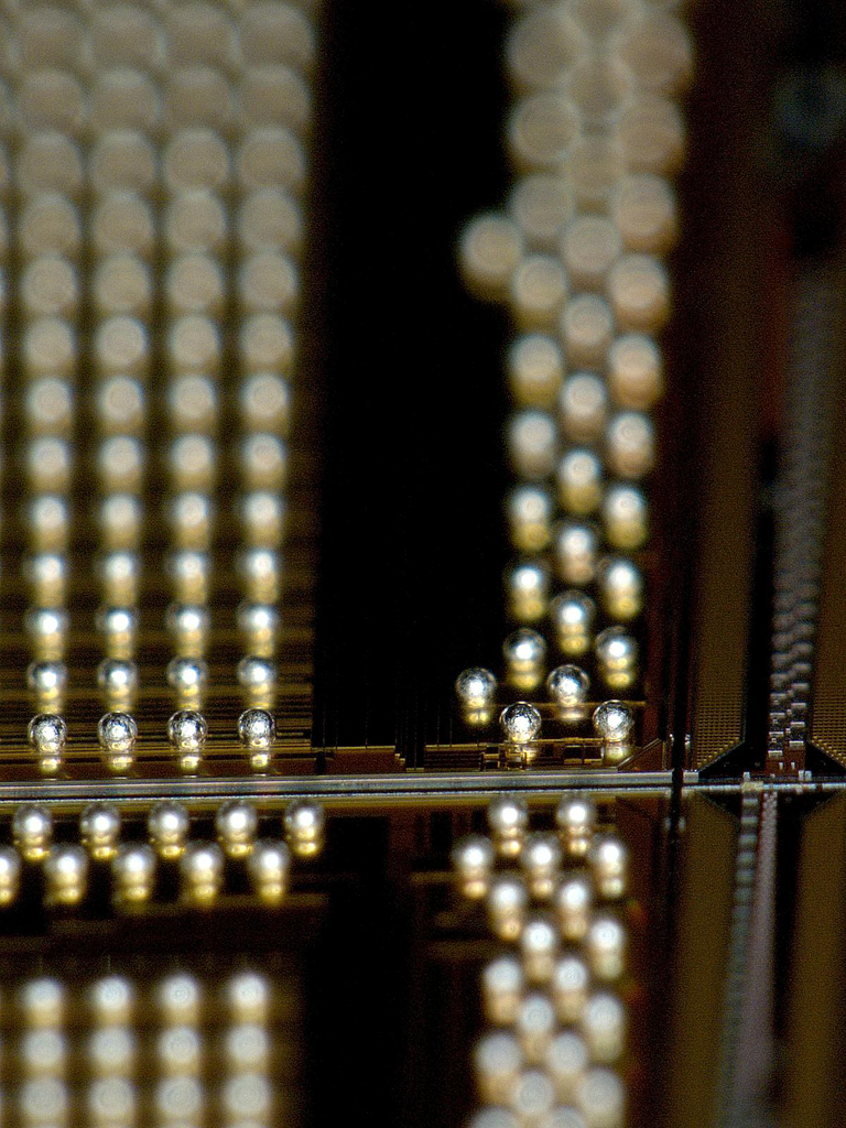
Detail of the solder balls deposited on top of the chips. The left part is the pixel matrix, the right part are the chip input/output connections.
Background: In some applications, the x-y-position of a 'light spot' containing a moderate number of photons must be identified. (The task which triggered this development is the detection of light from scintillating crystals in PET, see above.) The usual approach to obtain position information is to subdivide the sensitive area into many segments - often squares - which are small enough that light is spread over several elements. By measuring the light intensity in all elements, a mathematical interpolation can provide position information which is much better than the size of the elements. This approach, however, requires many elements - often SiPMs - and thus many electronics channels with need for power and cooling and producing a lot of data.
Project Description:
We have developed (and patented) a simple approach to make SiPM devices
intrinsically position sensitive for 'clusters' of photons.
The idea is inspired by the 'wedge-and-strip' idea used in some particle detectors.
In that approach, an electrode is cleverly
segmented
into 3 regions which are shaped such that the signals induced by a large signal 'blob' depends on position. Unfortunately, this only works,
if the blobs are big enough to always hit 3 pads.
The idea of the 'Interpolating Silicon Multiplier' ISiPM is to introduce 3-4 readout electrodes such that the signal generated
on each electrode by a photon cluster depends on the position. This achieved by a connecting the individual SPADs of the SiPM in such a way
to the electrode, that the local ratio follows a pre-defined function. This is best understood by the figure (left top) which shows
the SPADs of a SiPM and - by the color - to which of 4 outputs they are connected. In the upper left corner most SPADs are connected to the
upper left red output so that a photon cluster in that area produces most of its signal in the red electrode.
In contrast, an equal number of SPADs is connected to all 4 electrodes in the central part of the
device, so that a photon cluster in the middle produces equal amplitudes on all 4 outputs.
Overall, the position can be reconstructed as the center of gravity of the 4 corner signals (if a suited distribution function is used).
This approach does not need any additional devices (like resistive or capacitive dividers) on the SiPM and is therefore very simple
to implement. Obviously, the method only works if clusters are 'large enough', i.e. cover a sufficient number of SPADs such that interpolation works.
A SiPM device implementing this idea, designed in Heidelberg and fabricated by FBK ,
is shown (right top) with the 4 output signals accessible at the bond pads at the bottom.
One of the first tests of this device is shown (right bottom): Three LYSO crystals, wrapped in white PTFE foil, are standing on
arbitrary positions on the ISiPM device. They are illuminated by a radioactive source from the side to generate scintillation light.
A heat map of the reconstructed positions for a similar arrangement with 3×3 crystals in 2 mm pitch is shown (left bottom).
This nice measurement demonstrates an excellent spatial resolution even for rather small crystals. The idea is published
here.
Concept: Assignment of individual SPADs to 4 readout channels.
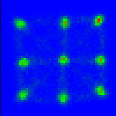
Successful measurement of the position of 3×3 LYSO crystals in 2 mm pitch.
Sensor as fabricated by FBK.
3 individual LYSO crystals (wrapped with PTFE) standing on a ISiPM device in a test setup.
- Contributions to the Belle-II vertex detector PXD: DEPFET steering chips ('Switcher'), readout chips ('DCD', I. Peric), module design, bump interconnect prototyping.
- Development of a readout chip for the detection of x-ray photons using a 2D APD matrix with time- and spatial resolution ('XNAP').
- Development of a system for fast spectrally resolved cell microscopy within the project Viroquant.
- Design of radiation tolerant circuits for application in particle detection.
- Low power, differential current mode logic for mixed signal applications.
- Circuits with very low transconductance for filters with very low corner frequencies.
- Analogue storage cells with very low droop.
- Protection of intellectual property: circuit design to generate reproducible secret tokens (Physically Unclonable Constant, PUC).
- Significant contribution to the design of the first pixel readout ASICs for ATLAS.
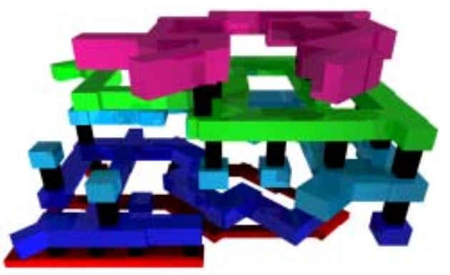
- Interactive 3D visualization of chip structures
3D illustration of simple chip structure.
Computer generated 3D capacitance structure used as PUC.
DCD Readout chip for Belle-II (and a smaller buffer chip) flip-chip mounted onto silicon substrate. The substrate is then wire bonded to a PCB for testing.